Method for establishing K-value and ten-value half adder and K-value and ten-value half subtracter based on band-pass threshold loading technology and circuit obtained based on method

A construction method and technology of a half-subtractor, applied in the direction of logic circuits with logic functions, etc., can solve the problems of large static power consumption, inability to change the threshold control characteristics, and high frequency performance degradation.

Inactive Publication Date: 2015-01-21
HEILONGJIANG UNIV
View PDF8 Cites 2 Cited by
  • Summary
  • Abstract
  • Description
  • Claims
  • Application Information

AI Technical Summary

Problems solved by technology

[0002] With the rapid development of MOS integrated circuit technology, the scale of integration is getting larger and higher, and VLSI (Very Large Scale Integration) has some shortcomings: ① First, on the VLSI substrate, the wiring takes up more than 70℅ of silicon chip area; in programmable logic devices, a large number of programmable internal wiring is also required to connect each logic function block or input/output to complete a specific function circuit, and wiring accounts for a large cost of materials
[0004] 1. In the realization of multi-valued circuits (K≥3), the existing semiconductor manufacturing process to control the threshold of MOS transistors has great disadvantages: ① The range of the control threshold is limited (due to the limited concentration of ion implantation), and the range of the control threshold in the process is often Change the performance of the MOS tube, and the realized voltage-type multi-valued circuit is not larger than the 4-valued circuit, and the application of more-valued circuits is difficult
② Only the magnitude of the threshold can be controlled, and the opening properties of the MOS tube cannot be changed (such as high-pass, low-pass, band-pass, band-resistance control threshold), and the multi-valued circuit must have a variety of MOS tubes with threshold-controlling properties to make the circuit structure most optimal. simple
③ It is necessary to add an additional process of ion implantation, and the threshold can only be controlled in the semiconductor manufacturing process, increasing the complexity of the process, and the threshold cannot be controlled by the user
[0005] 2. In the realization of multi-valued circuits, the existing neuron MOS transistor control threshold technology has great disadvantages: ① With the increase of K value, 'the input...

Method used


Image

  • Method for establishing K-value and ten-value half adder and K-value and ten-value half subtracter based on band-pass threshold loading technology and circuit obtained based on method
  • Method for establishing K-value and ten-value half adder and K-value and ten-value half subtracter based on band-pass threshold loading technology and circuit obtained based on method
  • Method for establishing K-value and ten-value half adder and K-value and ten-value half subtracter based on band-pass threshold loading technology and circuit obtained based on method

Examples


Embodiment 1

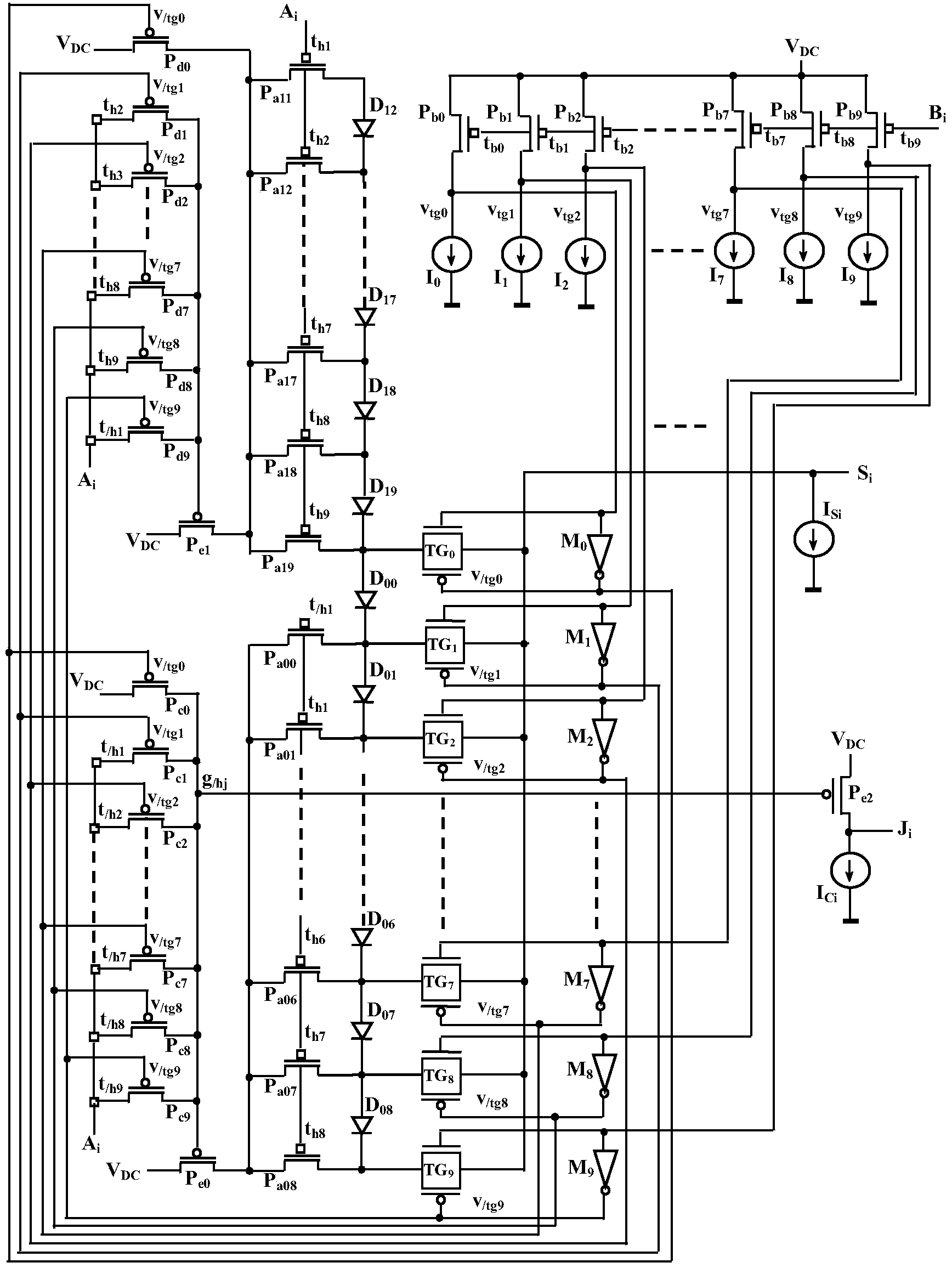
[0057] Embodiment 1: the proof that K value half subtractor of the present invention and half adder construction method feature are identical:

[0058] (1) K value half reducer features: A i is the minuend, B i is the subtrahend, S i Based on bad, J i is the number of borrowing digits, let A i =k,B i =j,

[0059] For the determined j=1~L, when ki =K+k-j>k, namely S i >A i ; When k=j, S i =0; when k>j and j≠L, S i =k-ji i , when j=L, there is no k>j; for a certain j=0, S i =A i ; For j≠0, when k

[0060] (2) K value half adder features: A i is the summand, B i is the addend, S i Based on harmony, C i is the carry number, let A i =k,B i =n, for a certain n, n=1~L, when k+ni =k+n>k, namely S i >A i , when k+n=K, S i =0, when k+n>K and n≠1, S i =k+n-Ki i , when n=1, there is no k+n>K; for certain n=0, S i =A i ; For n≠0, when k+n

Embodiment 2

[0064] Embodiment 2: K value half reducer S i Description of the output:

[0065] When j≠0 and k=1~j-1, the tube P e0 conduction, tube P e0 Drain voltage V Pe0 =V DC , the circuit in the low value area is invalid; when k=j-1, the tube P a0j-1 conduction, S i by TG j and P a0j-1 connected to V Pe0 , S i output voltage V Si =V DC , namely S i =L; when k=j-2, tube P a0j-2 、D 0j-1 conduction, tube P a0j-1 Cut off, S i by TG j ,P a0j-2 、D 0j-1 connected to V Pe0 , S i and V Pe0 There is a diode D between 0j-1 , V Si =V DC -VDon , namely S i =L-1; when k=j-3, tube P a0j-3 、D 0j-1 、D 0j-2 conduction, tube P a0j-1 and P a0j-2 Cut off, S i by TG j ,P a0j-3 、D 0j-1 、D 0j-2 connected to V Pe0 , S i and V Pe0 Between 2 diodes, V Si =V DC -2V Don , namely S i =L-2; ‥..., when k=1, tube P a01 、D 02 ~D 0j-1 conduction, tube P a02 ~P a0j-1 Cut off, S i by TG j ,P a01 、D 02 ~D 0j-1 connected to V Pe0 , S i and V Pe0 There are (j-2) diodes ...

Embodiment 3

[0069] Embodiment 3: Description of the PMOS transistor band-pass, high-pass and low-pass variable threshold circuit functions of the present invention:

[0070] Refer to [1] patent 201110291038.5 'PMOS tube band-pass-band-resistance and high-pass-low-pass variable threshold circuit' (invention content, drawings and embodiment 1, etc.), patent [2] 201110280921.4' 8-value storage embedded in DRAM storage matrix The 8-value information refreshing method of unit and related circuit' (accompanying drawing and embodiment 4 etc.), according to the characteristic variable threshold circuit of the present invention, describe as follows:

[0071] [1] PMOS tube with pass-variable threshold circuit: apply patent [1] or [2] Image 6 Redraw to the patent of the invention Figure 5 , where the PMOS transistor Q 2 , Q 4 , Q 5 , Q B1 in turn rewritten as P 2 ,P 4 ,P 5 ,P b1 , NMOS tube Q 1 , Q 3 in turn rewritten as N 1 , N 3 , V x rewritten as V in , remember v bx1 =V ex1 +V...


PUM

PropertyMeasurementUnit
Thicknessaaaaaaaaaa

Abstract

The invention discloses a method for establishing a K-value and ten-value half adder and a K-value and ten-value half subtracter based on the band-pass threshold loading technology and a circuit obtained based on the method. According to the method for establishing the K-value and ten-value half adder and the K-value and ten-value half subtracter based on the band-pass threshold loading technology and the circuit obtained based on the method, the band-pass threshold loading technology is adopted, the demands in all stages are processed according to information, and band-pass thresholds required in different stages are loaded to a PMOS tube, so that the band-pass threshold of the PMOS tube can be changed at any time; the K-value half subtracter and the half adder are analyzed, the characteristic that a high-value area and a low-value area are unified is realized, based on the loading technology, two kinds of circuits can be replaced by one kind of circuits, the traditional method achieved based on a K-value logic gate is avoided, and the circuit structure is simplified greatly; the chaotic encryption method and the circuit can be popularized to K values from two values, K-value multiplication and division are replaced by K-value addition and subtraction, and the multiplication-and-division-free chaotic encryption method and circuit for K-value information are obtained. The method for establishing the K-value and ten-value half adder and the K-value and ten-value half subtracter based on the band-pass threshold loading technology and the circuit obtained based on the method are applied to the VLSIs such as the FPGAs, CPLDs, half-custom or full-custom ASICs and memorizers and the technical field of other digital ICs.

Description

(1) Technical field [0001] The invention belongs to the field of digital integrated circuits, in particular to a construction method of a K-value and ten-value half-adder and half-subtractor using band-pass threshold loading technology and a circuit thereof. (2) Background technology [0002] With the rapid development of MOS integrated circuit technology, the scale of integration is getting larger and higher, and VLSI (Very Large Scale Integration) has some shortcomings: ① First, on the VLSI substrate, the wiring takes up more than 70℅ of silicon Chip area; in programmable logic devices, a large number of programmable internal wiring is also required to connect each logic function block or input / output to complete a specific function circuit, and wiring accounts for a large cost of materials. Reducing wiring costs becomes an important issue. ② From the perspective of information transmission, the use of multi-valued signals can reduce the number of connections; for each co...

Claims


Application Information

Patent Timeline
IPC IPC(8): H03K19/20
Inventor 方振贤刘莹方倩
Owner HEILONGJIANG UNIV
Why Eureka
Try Eureka