K-value and ten-value signal controlled data distributor and data selector

A technology of data distributor and data selector, which is applied in the direction of digital transmission system, safety communication device, pulse technology, etc., and can solve the problems of large hysteresis voltage, leakage of floating gate capacitance, control threshold, etc.

Inactive Publication Date: 2015-02-04
HEILONGJIANG UNIV
View PDF5 Cites 1 Cited by
  • Summary
  • Abstract
  • Description
  • Claims
  • Application Information

AI Technical Summary

Problems solved by technology

[0002] With the rapid development of MOS integrated circuit technology, the scale of integration is getting larger and higher, and VLSI (Very Large Scale Integration) has some shortcomings: ① First, on the VLSI substrate, the wiring takes up more than 70℅ of silicon chip area; in programmable logic devices, a large number of programmable internal wiring is also required to connect each logic function block or input / output to complete a specific function circuit, and wiring accounts for a large cost of materials
[0004] 1. In the realization of multi-valued circuits (K≥3), the existing semiconductor manufacturing process control MOS transistor threshold technology has great disadvantages: ① the range of control threshold is limited (because the ion implantation concentration is limited), and the control threshold in the process The amplitude often changes the performance of the MOS tube, and the voltage-type multi-valued circuit thus realized is not larger than the 4-valued circuit, and the application of more-valued circuits is difficult
② Only the amplitude of the threshold can be controlled, and the opening properties of the MOS tube cannot be changed (such as high-pass, low-pass, band-pass, and band-resistance 4 kinds of control thresholds), and the multi-value circuit must have 4 kinds of MOS tubes with threshold control properties to make the circuit Simplest structure
③ It is necessary to add an additional process of ion implantation, and the threshold can only be controlled in the semiconductor manufacturing process, which not only increases the complexity of the process, but also cannot be controlled by the user
[0005] 2. In the realization of multi-valued circuits, the existing neuron MOS transistor control threshold technology has great disadvantages: ① With the increase of K value, 'the input gate and control gate capacitance of a single neuron MOS transistor occupies the area of ​​the silicon chip' versus 'a single neuron MOS transistor'. The ratio of the MOS tube to the area of ​​the silicon chip is getting larger and larger, such as ten times, a hundred times or higher; ②As the K value increases, the width of the threshold fuzzy region (turning region) of the input gate ΔV 1 'to' Floating Gate Threshold Fuzzy Area (Turning Area) Width ΔV fg ’ ratio (ΔV 1 / ΔV fg =C TOT / C 1 ) is getting bigger and bigger, because ΔV fg is certain, the threshold fuzzy area ΔV of the input gate 1 The width is getting bigger and bigger, so that the input gate K value signal resolution ability is getting lower and lower, and the capacitance accuracy is high, which is not conducive to or cannot reliably realize the multi-valued circuit with large K value; ③The threshold control characteristics cannot be changed (such as with Pass-through and band-stop control threshold mode), which is unfavorable for simplifying the K value circuit; ④ With the increase of the K value, the ratio (C TOT / C 1 ) becomes larger, the capacitance of the input gate and the control gate increases, and the high-frequency performance decreases rapidly; ⑤ With the increase of the K value, the leakage of the floating gate capacitance cannot be omitted, and it is difficult to refresh the multi-valued information
⑥The static power consumption of the neuron CMOS inverter is 0 only for the binary signal. For a large K value, there is a state where the NMOS tube and the PMOS tube are turned on at the same time, and the static power consumption is even greater; the output of the neuron CMOS follower is usually Capacitive load, there is a period when the NMOS tube and the PMOS tube are cut off at the same time, the output voltage rises and falls on different tracks, and there is a large hysteresis voltage, which is not conducive to multi-valued circuits.

Method used


Image

  • K-value and ten-value signal controlled data distributor and data selector
  • K-value and ten-value signal controlled data distributor and data selector
  • K-value and ten-value signal controlled data distributor and data selector

Examples


Embodiment 1

[0036] Embodiment 1: Description of the PMOS tube band-pass, high-pass and low-pass variable threshold circuit functions of the present invention:

[0037] Refer to the relevant content of the following two patents: [1] Patent No. 201110291038.5 'PMOS tube bandpass-band-resistance and high-pass-low pass variable threshold circuit' (invention content, drawings and embodiment 1, etc.), [2] The patent No. 201110280921.4 is the patent '8-value information refreshing method and related circuit of 8-value storage unit embedded in DRAM memory matrix' (accompanying drawings and embodiment 4, etc.), according to the characteristics of the present invention, PMOS tube band-pass, high-pass and low-pass The variable threshold circuit is described as follows:

[0038] [1] PMOS tube with pass-variable threshold circuit: According to the characteristics of the patent of the present invention only using high pass-variable threshold circuit, at first patent [1] or [2] Figure 6 The band-pass-...

Embodiment 2

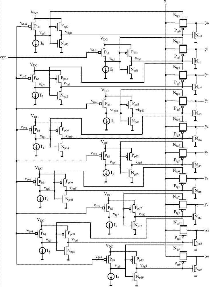
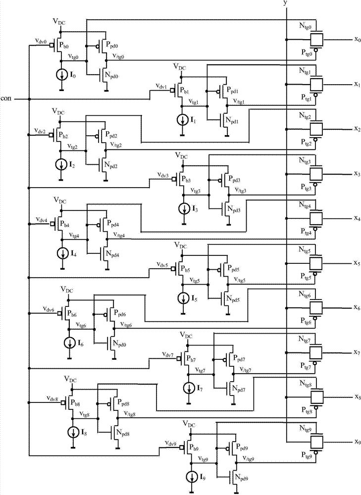
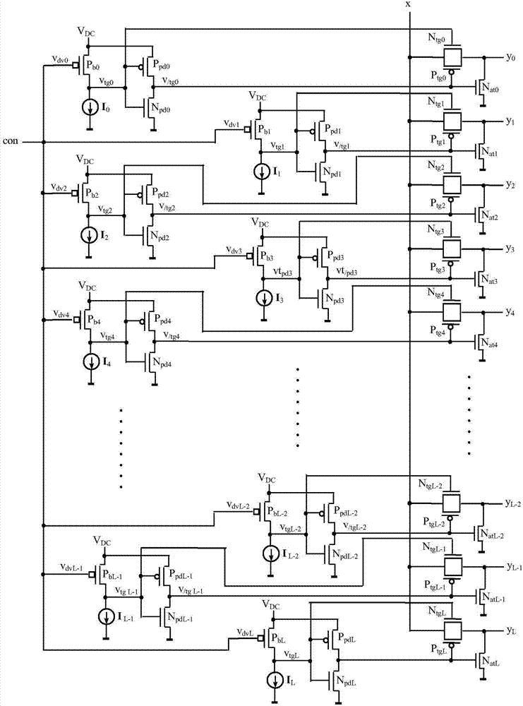
[0044] Embodiment 2: K logic value discrimination gate U 0 ~ U L instruction of:

[0045] K logical value discrimination gate U 0 ~ U L Among them, K-2 U 1 ~ U L-1 Respectively, K-2 band-pass variable threshold PMOS transistors P with the smallest intervals b1 ~P bL-1 And K-2 constant current sources I 1 ~I L-1 make up, u L A high-pass variable-threshold PMOS transistor P with the smallest interval bL and a constant current source I L make up, u 0 A low-pass variable-threshold PMOS transistor P with the smallest interval b0 and a constant current source I 0 Composition, the smallest low-pass, band-pass and high-pass variable threshold PMOS transistor P in all intervals b0 ~P bL The effective inputs of all are connected to the control input con; the logic value of the input con and x is i respectively expressed as con=i and x=i, the noise-free logic level of the input and output logic value i is called i level, con and x The i levels of x are denoted as V con (...

Embodiment 3

[0048] Example 3: to figure 1 and 2 Pspice computer simulation waveform Figures 9 to 14 instruction of.

[0049] figure 2 Be the circuit diagram of the data selector of 10 value signal control of the present invention; To figure 2 (10 value data selector) carry out Pspice computer simulation, ① draw at first Figure 9 , Figure 9 for figure 2 The circuit shown is under the action of the control input con, 10 data inputs x 0 ~x L The working waveform diagram transmitted to the data output y, the order of waveforms from top to bottom is: y, con, x 9 、x 8 、x 7 、x 6 、x 5 、x 4 、x 3 、x 2 、x 1 、x 0 ;Depend on Figure 9 It can be seen that when con is a stable 0 level, y=x 0 , that is, input x 0 Transfer to output y; when con is a stable 1 level, y=x 1 , namely x 1 Transfer to y; when con is a stable 2-level, y=x 2 , namely x 2 Transfer to y; when con is a stable 3-level, y=x 3 , namely x 3 Send to y;...; When con is a stable 8-level, y=x 8 , namely x ...


PUM


Abstract

The invention discloses a K-value and ten-value signal controlled data distributor and data selector. The K-value data distributor is composed of K CMOS transmission gates, K CMOS NOT gates, K logic value discrimination gates and K NMOS tubes. The K NMOS tubes of the K-value data distributor are deleted, and then input is changed into output and output is changed into input so that the K-value data selector is obtained. The K-value data selector and the distributor are important devices for changing a K-value data transmission channel. In order to popularize a chaotic encryption method and an encryption circuit from 2-value information to K-value information, the K-value data selector and the distributor can be used so that a K-value shift data selector is realized, K-value multiplication and division operation is substituted by addition and subtraction operation, and thus a no-multiplication-and-division chaotic encryption circuit of K-value information is realized. The data distributor and the data selector are applied to the technical fields of VLSI like FPGA, CPLD, semi-custom or full-custom ASIC and memories and other digital IC.

Description

(1) Technical field [0001] The invention belongs to the field of digital integrated circuits, in particular to a data distributor and a data selector controlled by K value and ten value signals. (2) Background technology [0002] With the rapid development of MOS integrated circuit technology, the scale of integration is getting larger and higher, and VLSI (Very Large Scale Integration) has some shortcomings: ① First, on the VLSI substrate, the wiring takes up more than 70℅ of silicon Chip area; in programmable logic devices, a large number of programmable internal wiring is also required to connect each logic function block or input / output to complete a specific function circuit, and wiring accounts for a large cost of materials. Reducing the proportion of wiring costs becomes a very important issue. ② From the perspective of information transmission, the use of multi-valued signals can reduce the number of connections; for each connection to transmit digital information, ...

Claims


Application Information

Patent Timeline
Patent Type & Authority Applications(China)
IPC IPC(8): H03K19/094H03K19/0948H04L9/00
Inventor 方振贤刘莹方倩
Owner HEILONGJIANG UNIV
Why Eureka
Try Eureka