Rapid optimization method for size of FPGA circuit transistors

A size optimization and transistor technology, applied in CAD circuit design, design optimization/simulation, electrical digital data processing, etc., can solve problems such as difficult to obtain the global optimal solution and affect product performance, so as to shorten optimization time and improve circuit design The effect of improving efficiency and reducing the number of combinations

Active Publication Date: 2018-02-27
FUDAN UNIV
View PDF2 Cites 2 Cited by
  • Summary
  • Abstract
  • Description
  • Claims
  • Application Information

AI Technical Summary

Problems solved by technology

If special circuit optimization technology is not used, it is difficult to obtain the glob...

Method used


Image

  • Rapid optimization method for size of FPGA circuit transistors
  • Rapid optimization method for size of FPGA circuit transistors
  • Rapid optimization method for size of FPGA circuit transistors

Examples


Embodiment Construction

[0027] The specific implementation is as follows:

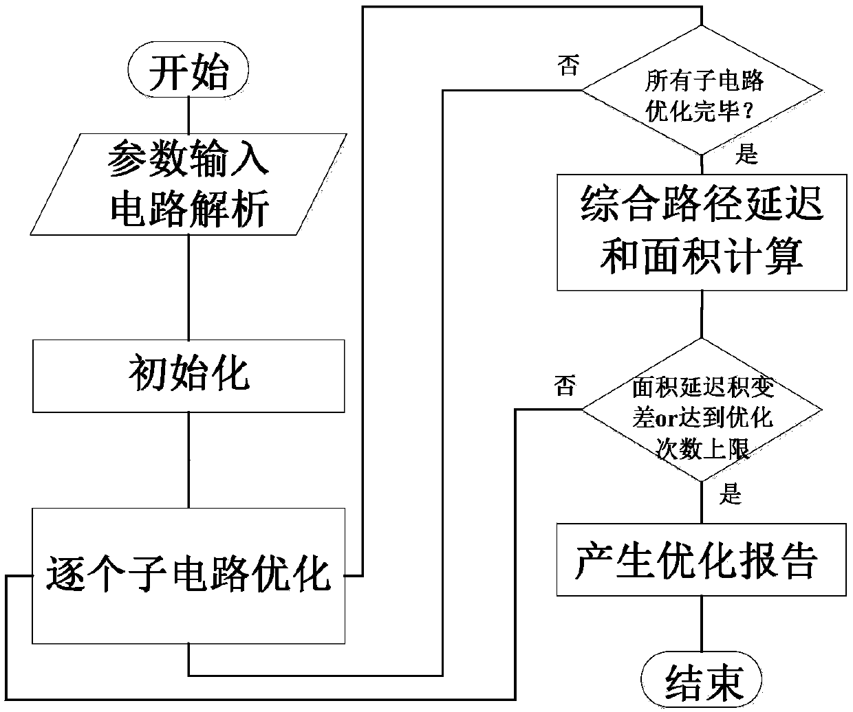
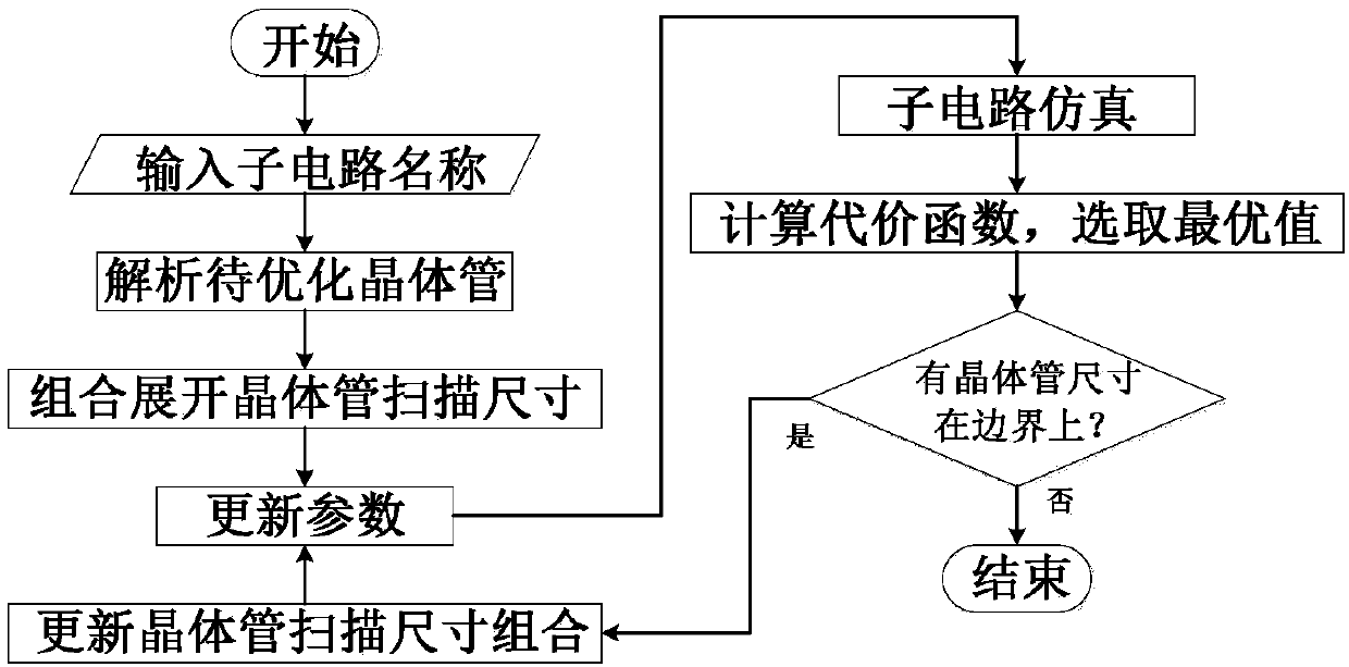
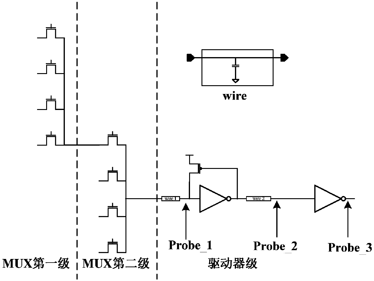
[0028] First, iterative optimization algorithms such as greedy algorithm, simulated fire algorithm, etc. are used. Here, the greedy algorithm is used as an example to perform traversal optimization on the transistors of each sub-circuit of the FPGA (such as figure 2 shown), here we take the double line sub-circuit as an example to illustrate, other circuits are similar. Such as image 3As shown in , the program first finds iso-optimized transistors in the subcircuit. Ptran_L1_nmos, Ptran_L2_nmos, inv_1_nmos, inv_1_pmos, inv_2_nmos, inv_2_pmos, rest_pmos a total of seven transistors. According to the greedy algorithm, it is necessary to expand the transistors to be optimized based on the existing values. For example, there are seven transistors in this example, and each transistor scans 5 values, then there are a total of 78125 (5 7 ) values, select the optimal value in this range, and check whether the optimal value is at...


PUM


Abstract

The invention belongs to the technical field of integrated circuits, and particularly relates to an optimization method for the size of FPGA circuit transistors. The method mainly includes the steps of conducting related sub-circuit analysis based on FPGA parameters, initializing the parasitic parameters of a circuit combined with FPGA circuit implement features, then conducting one-by-one optimization on each sub-circuit, after all the sub-circuits are optimized, conducting comprehensive optimization of delay and areas, and outputting an optimization result report file. According to the optimization method, a related algorithm can be adopted to improve the optimization quality and increase the optimization speed; for example, the modes such as bundled circuit combination optimization areadopted to decrease the optimization number of the transistors and increase the optimization speed; multithreaded acceleration runs to conduct parallelization treatment on some circuits without mutualcoupling relationships so as to accelerate the optimization process. By the optimization method, the optimization time of the size of the FPGA circuit transistors can be greatly shortened, and compared with a traditional full custom circuit, the circuit has design efficiency which is improved by more than 10 times.

Description

technical field [0001] The invention belongs to the technical field of integrated circuits, and in particular relates to a method for optimizing the transistor size of an FPGA circuit. Background technique [0002] FPAG is a regular array structure based on repeating units. It is this regular structure that makes it often the first to use the world's most cutting-edge IC technology and design technology. Its integration ranks among the best in various ICs, reaching tens of billions of transistors. This kind of regular FPGA circuit generally adopts a full-custom design method to obtain its high performance [1-4]. However, due to the size selection and interrelated coupling between the circuit modules that make up its different functions, the usual ASIC full-custom design technology is applied to such a large FPGA circuit. When the capacity FPGA circuit is used, the optimization space is very limited. If special circuit optimization technology is not used, it is difficult to ...

Claims


Application Information

Patent Timeline
IPC IPC(8): G06F17/50
CPCG06F30/20G06F30/34
Inventor 来金梅陈威同王健
Owner FUDAN UNIV
Why Eureka
Try Eureka