Bifacial circuit board surface assembly process

A double-sided circuit board and assembly process technology, applied in the direction of assembling printed circuits with electrical components, can solve the problems of large thermal shocks of printed circuit boards, many ICT misjudgments, and damage to printed circuit boards and components on them. Small, less oxidation, less thermal shock effect

Inactive Publication Date: 2009-09-09
MITAC COMP (SHUN DE) LTD
View PDF0 Cites 16 Cited by
  • Summary
  • Abstract
  • Description
  • Claims
  • Application Information

AI Technical Summary

Problems solved by technology

[0003] The above-mentioned traditional double-sided surface assembly process requires two reflow furnaces, which has a large thermal impact on the printed circuit board, which seriously affects the tinning of the components on the second side of the assembled printed circuit board and the rear-end plug-in components, resulting in many ICT misjudgments. , and during the midway turnover, it is easy to cause damage to the printed circuit board and its components

Method used


Image

  • Bifacial circuit board surface assembly process

Examples


Embodiment Construction

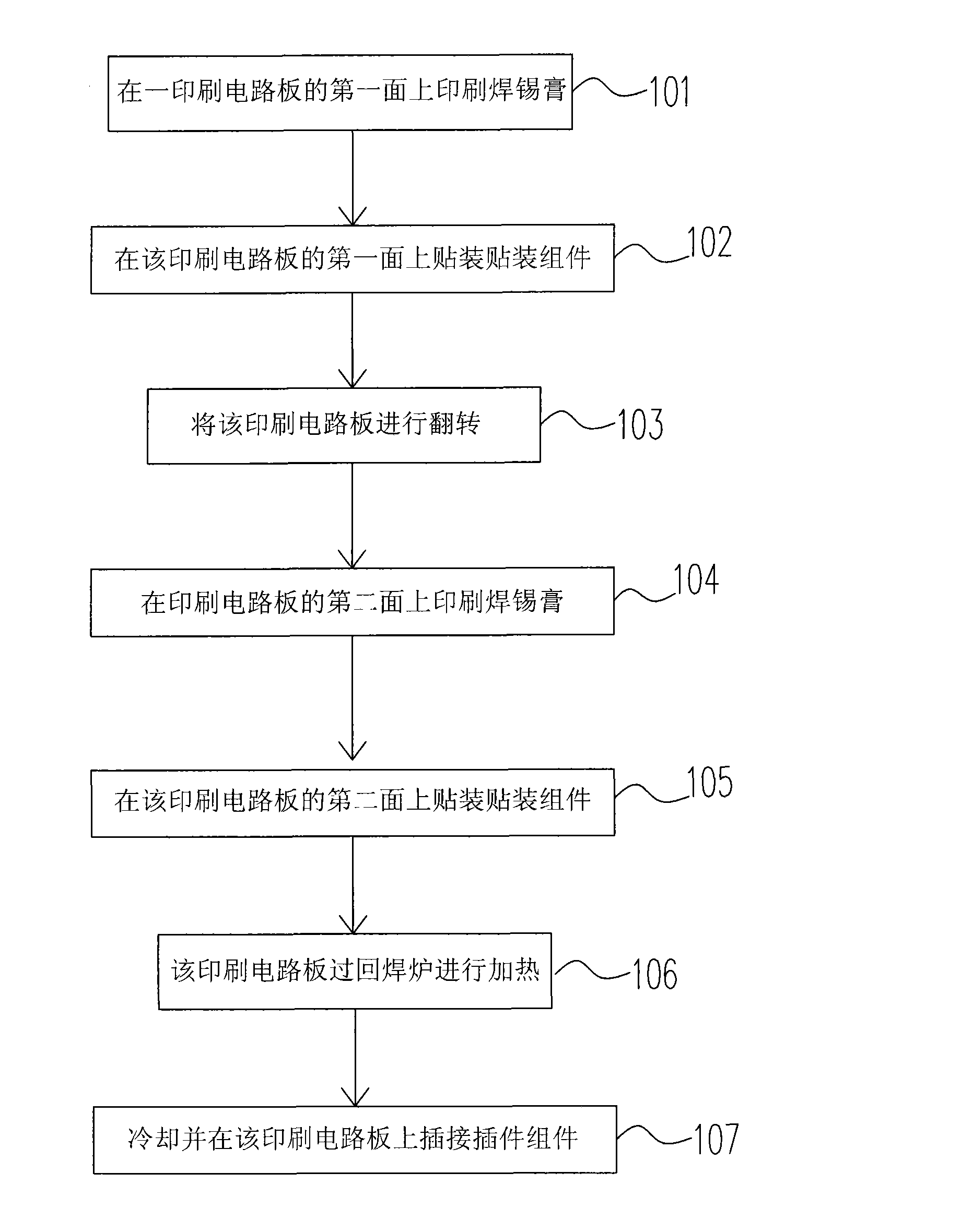
[0014] Please refer to figure 1 As shown, it is a schematic flow chart of the surface assembly process of the double-sided circuit board described in the present invention.

[0015] The surface assembly process of the double-sided circuit board of the present invention mainly includes the following steps:

[0016] Step 101: printing solder paste on the first surface of a printed circuit board;

[0017] Step 102: mounting a mounting component on the first surface of the printed circuit board printed with solder paste;

[0018] Step 103: Turn over the printed circuit board by using a turning machine;

[0019] Step 104: After the printed circuit board is turned over, print solder paste on the second surface of the printed circuit board;

[0020] Step 105: Mounting mounting components on the second surface of the printed circuit board;

[0021] Step 106: using a reflow furnace to heat the first surface and the second surface of the above-mentioned printed circuit board until t...


PUM


Abstract

The invention provides a bifacial circuit board surface assembly process, wherein the process mainly comprises the following steps: firstly, assembling assembly parts on the first surface of a printed circuit board printed with solder paste; secondly, overturning the printed circuit board by a tilter, assembling the assembly parts on the second surface of the printed circuit board printed with the solder paste; thirdly, passing the assembled printed circuit board through a reflow oven, and welding the assembled parts on the printed circuit board; and finally, inserting plug-in assembly parts in the printed circuit board. In the bifacial circuit board surface assembly process of the invention, the printed circuit board only passes through the reflow oven once, the printed circuit board has the advantages of less heat shock, less oxygenation, no circular flow and less printed circuit board damage.

Description

technical field [0001] The invention relates to an assembly process, in particular to a surface assembly process of a circuit board. Background technique [0002] The traditional double-sided circuit board surface assembly process (Surface Mounted Technology hereinafter referred to as SMT), the surface assembly process is to assemble the first side of the printed circuit board on one SMT line, and then transfer to another line after passing through the reflow oven. The SMT line or the SMT line is then assembled on the second side of the printed circuit board. After the assembly is completed, the printed circuit board still needs to go through a reflow furnace, and finally the plug-in components are inserted on the printed circuit board. [0003] The above-mentioned traditional double-sided surface assembly process requires two reflow furnaces, which has a large thermal impact on the printed circuit board, which seriously affects the tinning of the components on the second si...

Claims


Application Information

Patent Timeline
Patent Type & Authority Applications(China)
IPC IPC(8): H05K3/30H05K3/34
Inventor 张泉淼
Owner MITAC COMP (SHUN DE) LTD
Why Eureka
Try Eureka