Check patentability & draft patents in minutes with Patsnap Eureka AI!

Electrode structure of memory capacitor and method for manufacturing memory capacitor structure

A technology of electrode structure and manufacturing method, applied in semiconductor/solid-state device manufacturing, circuits, electrical components, etc., can solve the problems of unstable capacitor structure, contact phenomenon, etc., to increase the surface area of ​​the capacitor, not easy to contact short circuit, and improve the capacitance Effect

Active Publication Date: 2009-09-23
IND TECH RES INST
View PDF4 Cites 4 Cited by
  • Summary
  • Abstract
  • Description
  • Claims
  • Application Information

AI Technical Summary

Problems solved by technology

For example, in the 90nm process, there may be contact phenomenon due to the instability of the capacitor structure

Method used


Image

  • Electrode structure of memory capacitor and method for manufacturing memory capacitor structure
  • Electrode structure of memory capacitor and method for manufacturing memory capacitor structure
  • Electrode structure of memory capacitor and method for manufacturing memory capacitor structure

Examples


Embodiment Construction

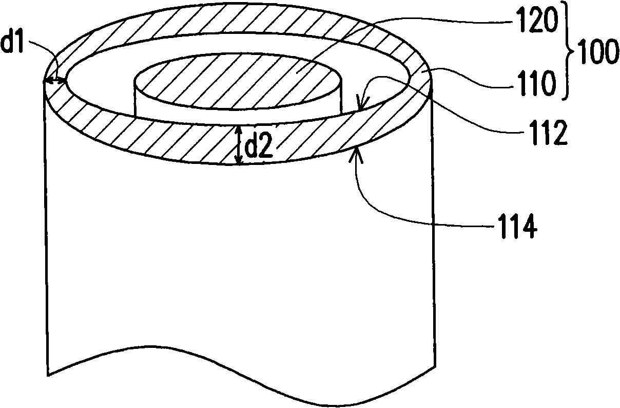
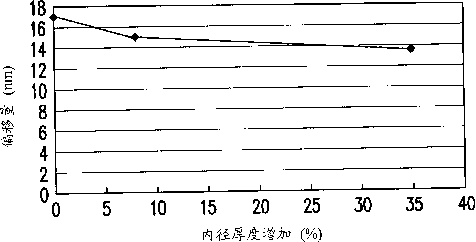
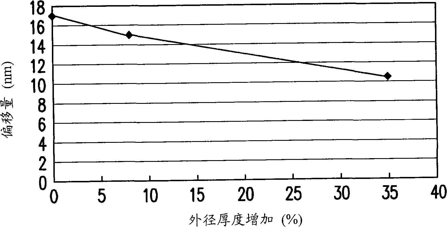
[0029] figure 1 It is a three-dimensional schematic diagram of an electrode structure of a memory capacitor according to an embodiment of the present invention, and FIG. 2 is a graph showing the influence of the thickness variation of the lower electrode on the strength of the capacitor structure.

[0030] Please refer to figure 1 , the lower electrode 100 of the storage capacitor is a composite electrode structure composed of an outer annular tube 110 and a central cylinder 120 . The radial section of the outer annular tube body 110 is elliptical, and has a thickness d1 along the major axis and a thickness d2 along the minor axis. In order to improve the structural displacement strength, the outer annular tube body 110 adopts an elliptical cross-section design, which can effectively reduce the probability of capacitance displacement compared with known cylindrical capacitors with weak structures. In addition, when fabricating the lower electrode 100 of the storage capacitor...


PUM


Abstract

The invention discloses an electrode structure of a memory capacitor and a method for manufacturing a memory capacitor structure. In a random access memory, due to process shrink, the surface area of a stacked capacitor is greatly reduced to influence the capacitance to fall so as to cause that the capacitor cannot work normally. The invention conceives that the surface area of the capacitor is increased by adopting a composite lower electrode of an external annular tube body and a central cylinder body with concave-convex surfaces in a limited memory unit area so as to further improve the capacitance. The radial section of the external annular tube body is elliptic, and the thickness in the elliptic short shaft direction is thickened so as to enhance the strength of the capacitor structure.

Description

technical field [0001] The invention relates to a semiconductor element and a manufacturing method thereof, and in particular to an electrode structure of a storage capacitor and a manufacturing method of the storage capacitor structure. Background technique [0002] With the advancement of technology, the application of semiconductor components is more and more extensive, such as dynamic random access memory (Dynamic Random Access Memory, DRAM) components or static random access memory (Static Random Access Memory, SRAM) Semiconductor storage elements such as devices generally include capacitors and transistors for storing and reading data or information. As the storage space required by the computer grows rapidly, the number of required capacitors and the capacitance of each capacitor also increase accordingly. Therefore, in order to meet such demands, semiconductor process technology must be changed in process technology. [0003] At the same time, in order to further i...

Claims


Application Information

Patent Timeline
Patent Type & Authority Applications(China)
IPC IPC(8): H01L27/108H01L21/8242H01L21/02H10B12/00
Inventor 陆苏财陈文华郑仙志陈韻巧
Owner IND TECH RES INST
Features
  • R&D
  • Intellectual Property
  • Life Sciences
  • Materials
  • Tech Scout
  • Unparalleled Data Quality
  • Higher Quality Content
  • 60% Fewer Hallucinations
Learn More