Thin film transistor substrate and manufacturing process thereof

A technology of thin film transistor and manufacturing process, applied in the field of thin film transistor substrate and its manufacturing process, can solve the problems of low aperture ratio of thin film transistor substrate and the like

Inactive Publication Date: 2009-09-23
INNOCOM TECH SHENZHEN +1
View PDF0 Cites 16 Cited by
  • Summary
  • Abstract
  • Description
  • Claims
  • Application Information

AI Technical Summary

Problems solved by technology
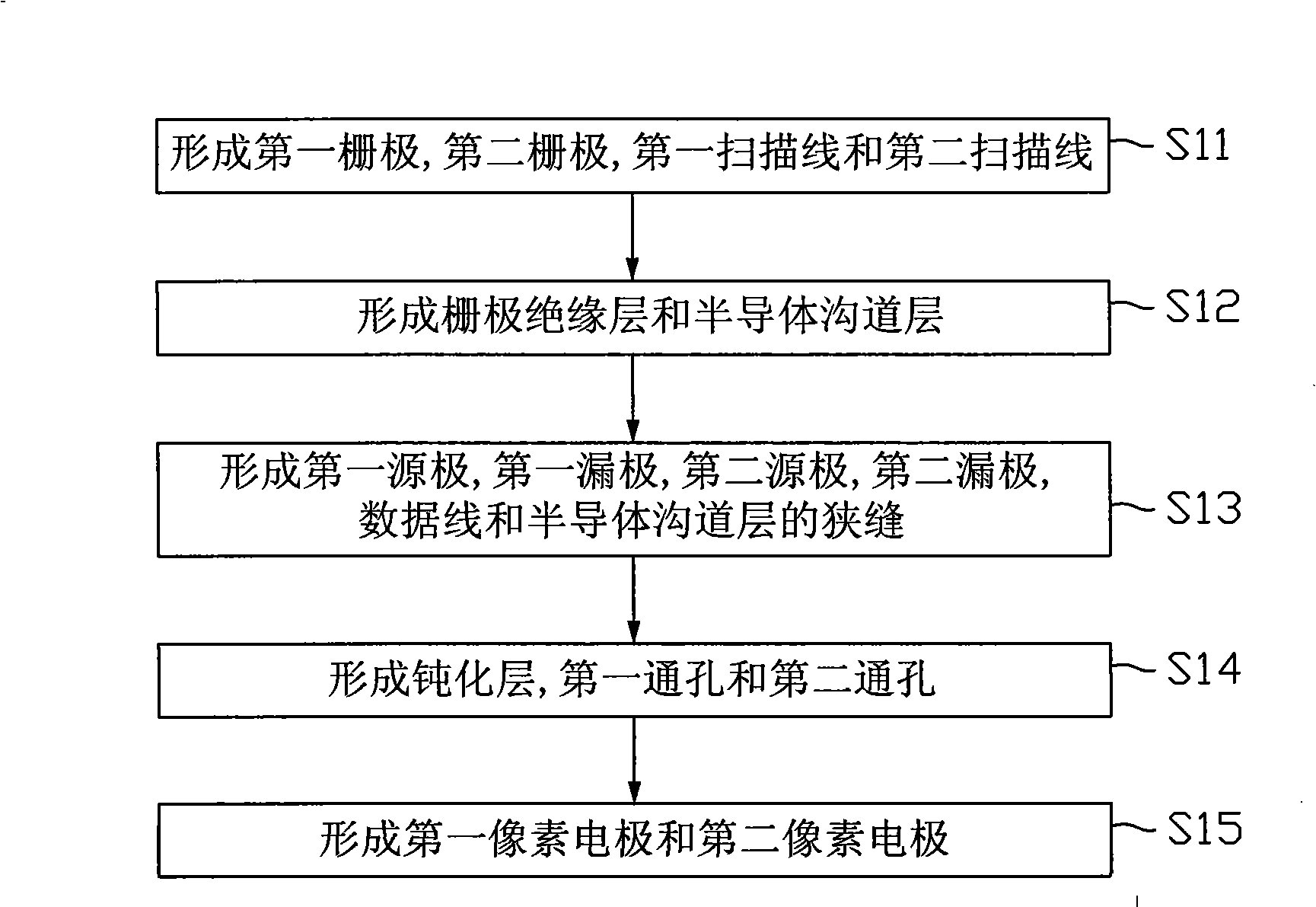
[0019] In order to solve the problem of the low aperture ratio of the thin film transistor substrate in the prior art, it is necessary to provide a thin film transistor substrate with a higher aperture ratio
[0020] In order to solve the problem of the low aperture ratio of the thin film transistor substrate obtained by the manufacturing process of the thin film transistor substrate in the prior art, it is necessary to provide a manufacturing process of the thin film transistor substrate that can obtain a higher aperture ratio

Method used


Image

  • Thin film transistor substrate and manufacturing process thereof
  • Thin film transistor substrate and manufacturing process thereof
  • Thin film transistor substrate and manufacturing process thereof

Examples


Embodiment Construction

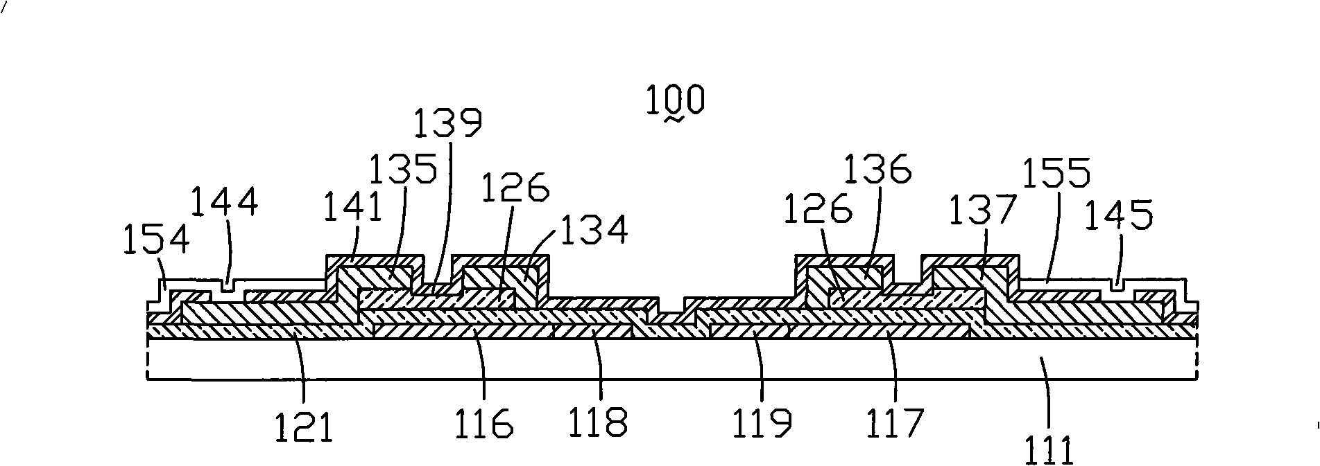
[0031] refer to Figure 4 , is a partial plan view of a preferred embodiment of the thin film transistor substrate of the present invention. The thin film transistor substrate 200 includes a plurality of first scan lines 218, a plurality of second scan lines 259, a plurality of data lines 238, a plurality of first thin film transistors 201, a plurality of second thin film transistors 203, and a plurality of first pixel electrodes 254 , a plurality of second pixel electrodes 255 , a plurality of first through holes 244 , a plurality of second through holes 245 and a plurality of third through holes 246 .

[0032]The plurality of first scan lines 218 are parallel to each other, the plurality of second scan lines 259 are parallel to the first scan lines 218, the second scan lines 259 correspond to the first scan lines 218 one-to-one and two corresponding scans The wires 218, 259 are insulated and overlapped. Wherein, the second scan line 259 is located directly above the first ...


PUM


Abstract

The invention relates to a thin film transistor substrate and a manufacturing process thereof. The thin film transistor substrate comprises a plurality of first scanning beams, second scanning beams, data wires, first pixel electrodes, second pixel electrodes, first thin film transistors and second thin film transistors. The first scanning beams are parallel with each other, the second scanning beams are parallel with the first scanning beams as well as insulated and overlapped with the first scanning beams; and the data wires are vertically insulated and crossed with the first scanning beams and the second scanning beams. Grids of the first thin film transistors are connected to the first scanning beams, source electrodes are connected to the data wires, and drain electrodes are connected to the first pixel electrodes; and grids of the second thin film transistors are connected to the second scanning beams, source electrodes are connected to the data wires, and drain electrodes are connected to the second pixel electrodes. The thin film transistor substrate has a high aperture opening ratio.

Description

technical field [0001] The invention relates to a thin film transistor substrate and a manufacturing process thereof. Background technique [0002] A liquid crystal display panel usually includes a thin film transistor substrate, a color filter substrate and a liquid crystal layer sandwiched between the two substrates, which realizes light by controlling the twisting of the liquid crystal molecules between the two substrates by applying voltages respectively. Pass or fail, so as to achieve the purpose of display. The liquid crystal driving method of the traditional liquid crystal display panel is the twisted nematic mode, but its viewing angle range is relatively narrow, that is, when the picture is observed from different angles, different display effects will be observed. [0003] In order to solve the problem of the narrow viewing angle of the twisted nematic mode liquid crystal display panel, the industry proposes a four-domain vertical alignment type liquid crystal dis...

Claims


Application Information

Patent Timeline
Patent Type & Authority Applications(China)
IPC IPC(8): H01L27/12H01L23/522H01L21/84H01L21/768G02F1/1362
Inventor 洪文明林育正陈建丞陈鹊如吴勇勋
Owner INNOCOM TECH SHENZHEN
Why Eureka
Try Eureka