Semiconductor integrated circuit

A technology of integrated circuits and semiconductors, which is applied in the direction of semiconductor devices, circuits, semiconductor/solid-state device components, etc., and can solve problems such as reduced integration and increased chip area

Inactive Publication Date: 2009-09-30
NEC ELECTRONICS CORP
View PDF2 Cites 2 Cited by
  • Summary
  • Abstract
  • Description
  • Claims
  • Application Information

AI Technical Summary

Problems solved by technology

If it is necessary to ensure the degree of freedom of wiring for signal wiring, it may lead to a decrease in integration and an increase in chip area

Method used


Image

  • Semiconductor integrated circuit
  • Semiconductor integrated circuit
  • Semiconductor integrated circuit

Examples


Embodiment 1

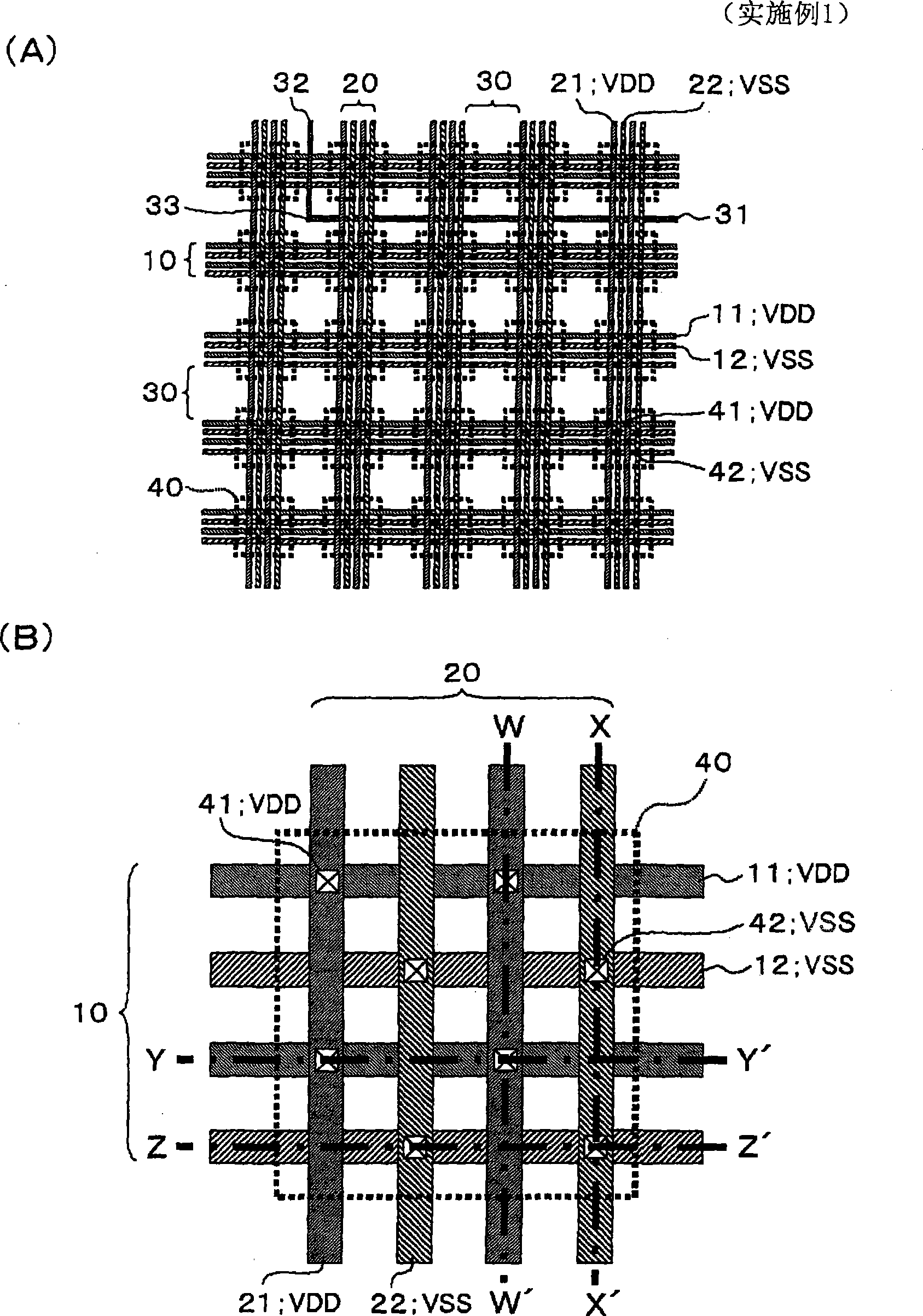
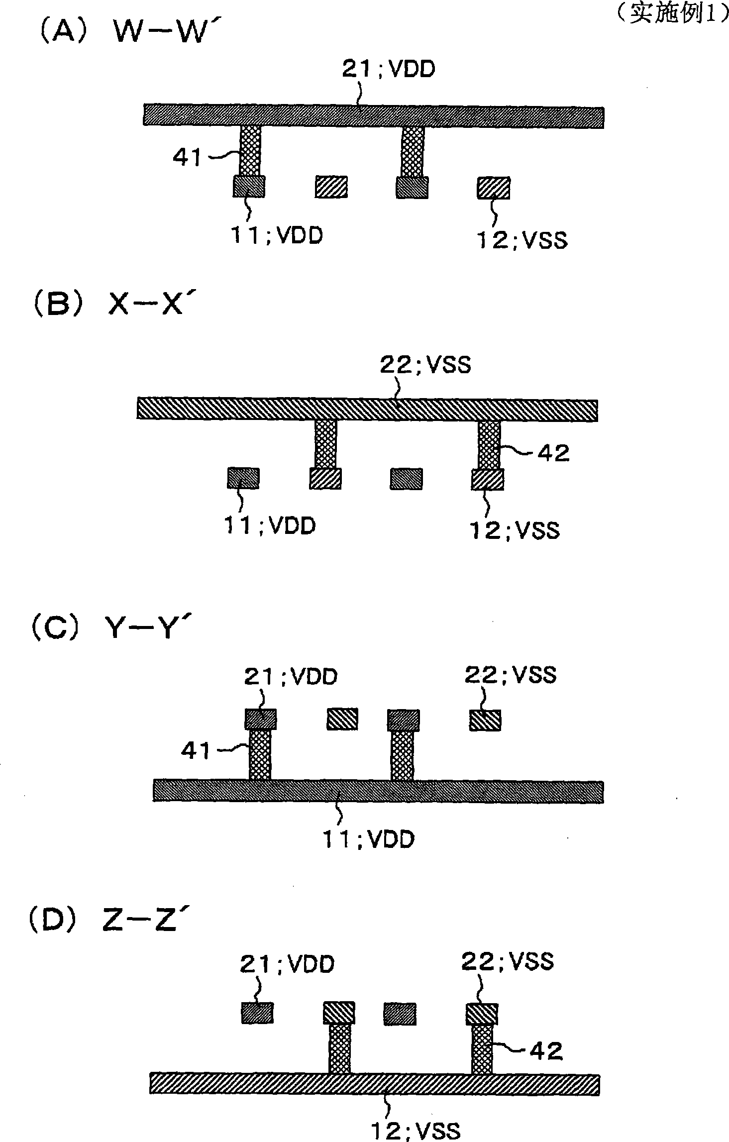
[0015] A semiconductor integrated circuit according to Embodiment 1 of the present invention will be described using the drawings. figure 1 It is (A) a partial plan view schematically showing the wiring structure of the semiconductor integrated circuit according to Embodiment 1 of the present invention and (B) an enlarged plan view of a three-dimensional intersection region. figure 2 It is a cross-sectional view between (A) W-W', (B) a cross-sectional view between XX', and a cross-sectional view between (C) Y-Y', schematically showing the wiring structure of the semiconductor integrated circuit according to Embodiment 1 of the present invention. , (D) Sectional view between Z-Z'. in addition, figure 1 and figure 2 Insulation layer is omitted.

[0016] refer to figure 1 , in a semiconductor integrated circuit, there are multilayer wiring layers on the elements formed on the semiconductor substrate, in which insulating layers and wiring layers are alternately stacked, a...


PUM


Abstract

Design rule violation regarding via density is avoided without decline in integration or an increase in chip area. Power wiring comprises a first-layer power wiring cluster in which VDD wiring trace and VSS wiring trace of different potentials at single trace width are arranged alternatingly; a second-layer power wiring cluster, disposed in a layer overlying the first-layer power wiring cluster, in which a VDD wiring trace and a VSS wiring trace of different potentials at single trace width are arranged alternatingly; and vias, placed in areas where the first-layer power wiring cluster and second-layer power wiring clusters intersect three-dimensionally, for electrically connecting wiring traces of the same potential in the first-layer power wiring cluster and wiring traces of the same potential in the second-layer power wiring cluster. A signal-wiring formation area is provided between mutually adjacent first-layer power wiring clusters and between mutually adjacent second-layer power wiring clusters.

Description

technical field [0001] The present invention relates to a semiconductor integrated circuit, and more particularly, to a semiconductor integrated circuit having bundle wiring in which wirings having a single wiring width are arranged at predetermined intervals. Background technique [0002] Wiring in a semiconductor integrated circuit is arranged according to predetermined design rules, and when the wiring is a multilayer wiring structure, the wiring layers are electrically connected through via holes. In such a multilayer wiring structure, in order to reduce the influence of the voltage drop, the power supply wiring and the ground wiring generally use wiring (thick wiring) wider than the width of the signal wiring, or use bundled wiring as follows, and arrange them in parallel at predetermined intervals. There is a single-wiring width substantially the same as that of the signal wiring. In addition, when there are two types of power supply lines (VDD line, VSS line) with di...

Claims


Application Information

Patent Timeline
Patent Type & Authority Applications(China)
IPC IPC(8): H01L23/528
CPCH01L23/5286H01L2924/0002H01L2924/00
Inventor 寺山俊明
Owner NEC ELECTRONICS CORP
Why Eureka
Try Eureka