Solid-state imaging device and manufacturing method thereof, and electronic apparatus and manufacturing method thereof

一种固体摄像元件、制造方法的技术,应用在电固体器件、电气元件、半导体器件等方向,能够解决不能角度修正等问题

Inactive Publication Date: 2009-09-30
SONY CORP
View PDF7 Cites 17 Cited by
  • Summary
  • Abstract
  • Description
  • Claims
  • Application Information

AI Technical Summary

Problems solved by technology

That is, if the angle exceeds a certain angle, the on-chip lens will not be able to correct the angle

Method used


Image

  • Solid-state imaging device and manufacturing method thereof, and electronic apparatus and manufacturing method thereof
  • Solid-state imaging device and manufacturing method thereof, and electronic apparatus and manufacturing method thereof
  • Solid-state imaging device and manufacturing method thereof, and electronic apparatus and manufacturing method thereof

Examples


Embodiment Construction

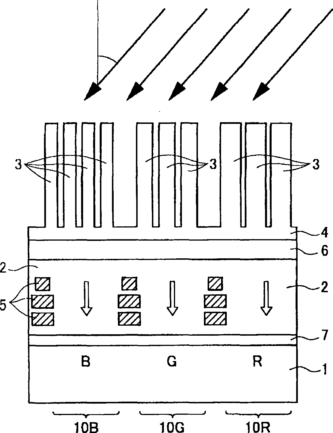
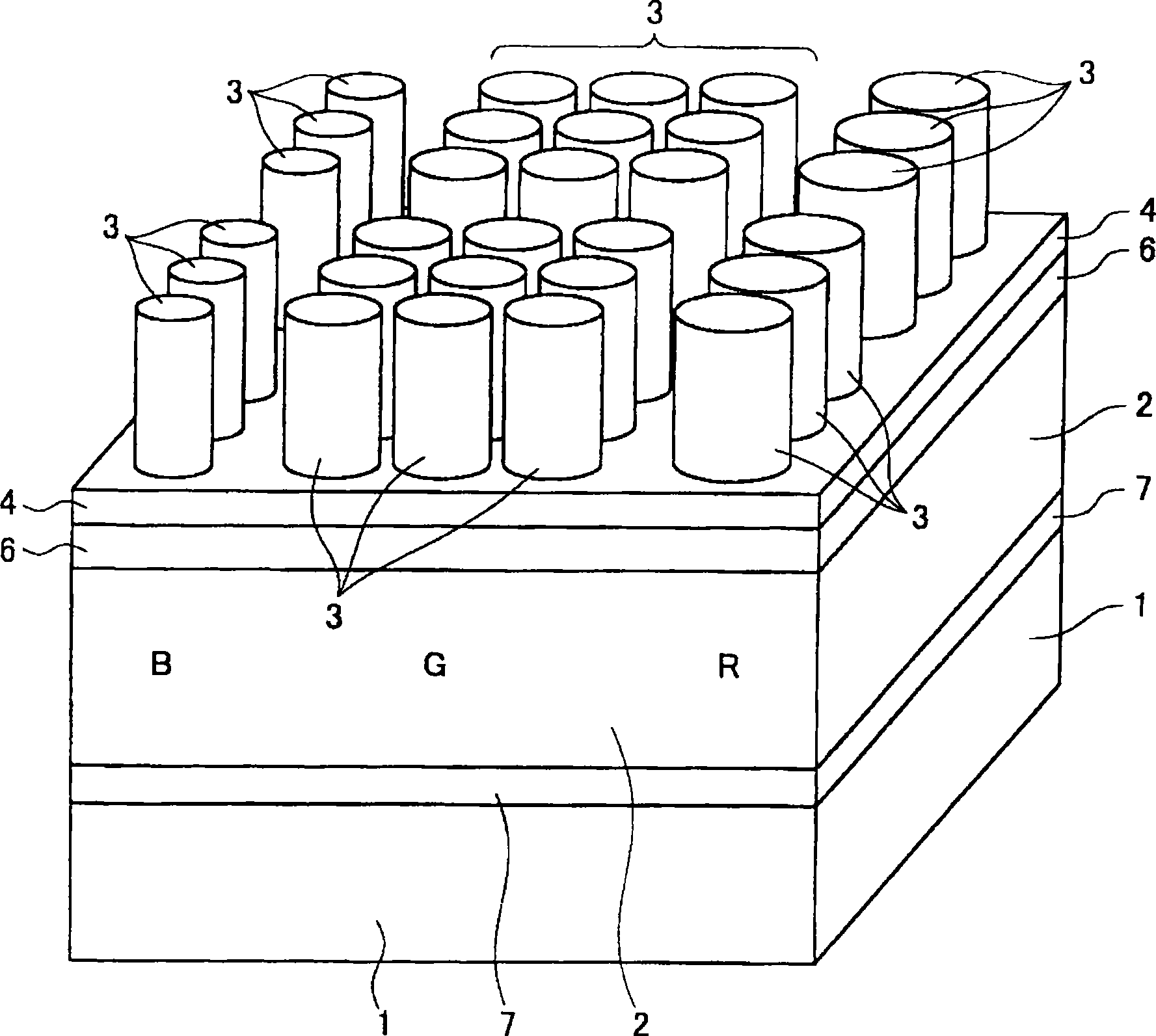
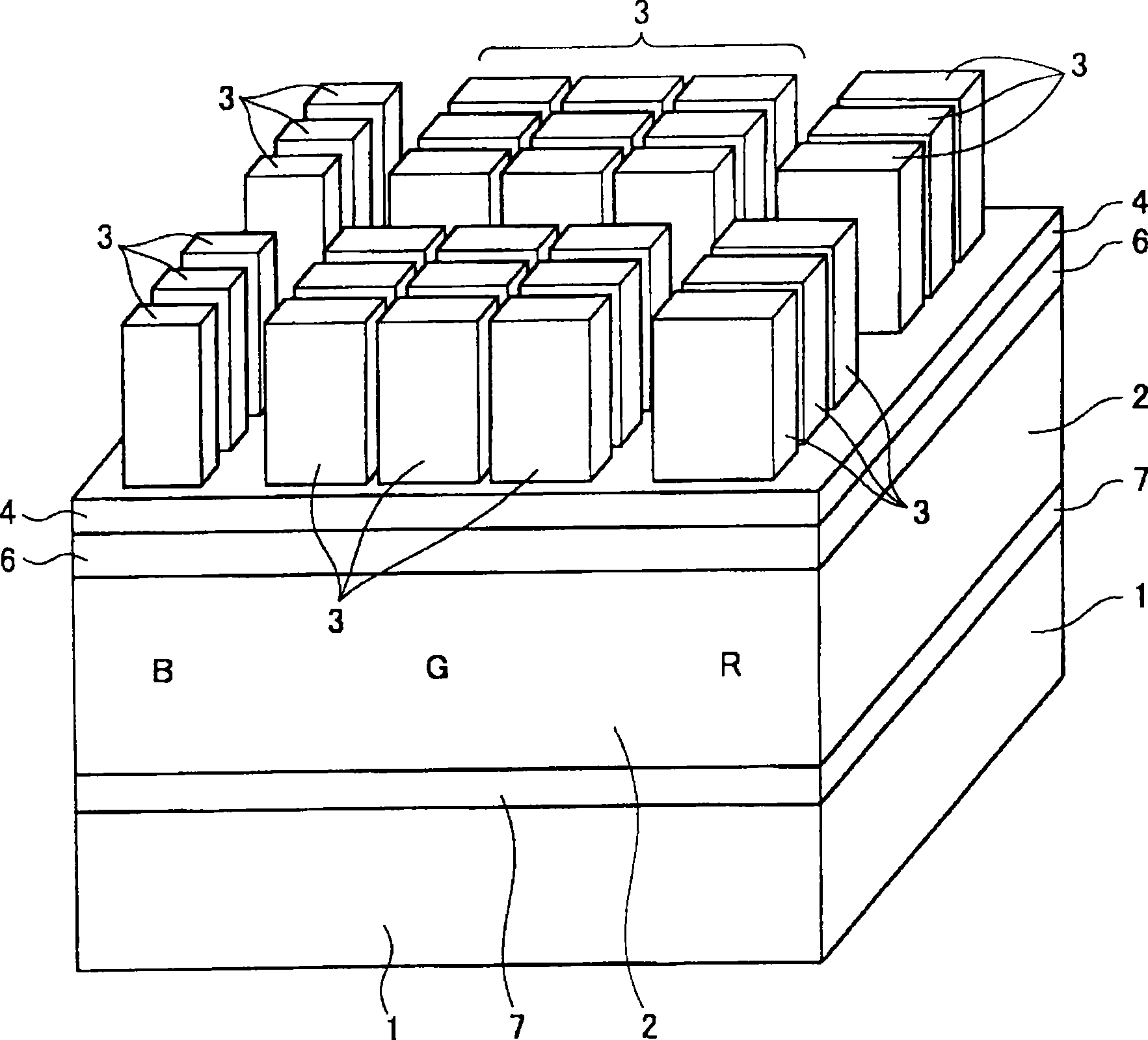
[0070] First, the outline of the present invention will be described before describing the specific embodiments of the present invention.

[0071] In the solid-state imaging device and electronic device of the present invention, a rod-shaped (rod-shaped) member made of a light-transmitting material is provided on each pixel instead of an on-chip lens. The rod-shaped member is a member for guiding incident light to a light receiving portion such as a photodiode, and is made of a light-transmitting material.

[0072] Here, with Figure 15 In the same manner as shown, the operation when light is obliquely incident is compared in the structure provided with the conventional on-chip lens and the structure provided with the rod-shaped member of the present invention, and is shown in Figure 4 .

[0073] Figure 4 (A) represents a conventional structure provided with an on-chip lens, Figure 4 (B) shows the structure provided with the rod-shaped member of this invention. The widt...


PUM


Abstract

The present invention provides a solid-state imaging device and manufacturing method thereof and electronic apparatus and manufacturing method thereof, the color can not be mixed even the pixel size is reduced. The solid-state imaging device of the invention includes a substrate (silicon substrate) 1 having a light receiving part for each of pixels (10B, 10G, 10R); and one or more rod members (3) made of a light transmissive material above the light receiving part for each of the pixels (10B, 10G, 10R).

Description

technical field [0001] The present invention relates to a solid-state imaging element, a manufacturing method thereof, electronic equipment, and a manufacturing method of the electronic equipment. Background technique [0002] Image sensors are devices used in a wide range of fields such as video cameras and video cameras. [0003] The image sensors used in these devices consist of many pixels. Moreover, the overall efficiency of the device depends on the size of the pixel and the pixel structure. [0004] In a color device, by providing each pixel with a solid-state absorbing filter material generally made of an organic material, the types of pixels can be classified into three colors: red, green, and blue. [0005] To improve the efficiency within a pixel, a pixel-sized lens is usually used. This is to ensure that the focus of incoming light is on the photosensitive element of the pixel, so that the pixel captures as much light as can be incident on the pixel without spr...

Claims


Application Information

Patent Timeline
Patent Type & Authority Applications(China)
IPC IPC(8): H01L27/146H01L27/14H04N5/335H04N5/357H04N5/369
CPCH01L27/14621H01L27/14627H01L27/14629H01L27/146
Inventor 约翰·伦尼
Owner SONY CORP
Why Eureka
Try Eureka