Methods for forming multiple-layer electrode structures for silicon photovoltaic cells

A technology of electrode structure and photovoltaic cells, applied in photovoltaic power generation, circuits, electrical components, etc.

Inactive Publication Date: 2009-09-30
PALO ALTO RES CENT INC
View PDF8 Cites 14 Cited by
  • Summary
  • Abstract
  • Description
  • Claims
  • Application Information

AI Technical Summary

Problems solved by technology

However, several issues associated with the use of printed nanophase metal inks to fill contact openings include: the quality and availability of the nanophase metal inks, the wetting behavior a...

Method used


Image

  • Methods for forming multiple-layer electrode structures for silicon photovoltaic cells
  • Methods for forming multiple-layer electrode structures for silicon photovoltaic cells
  • Methods for forming multiple-layer electrode structures for silicon photovoltaic cells

Examples


Embodiment

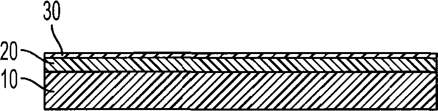
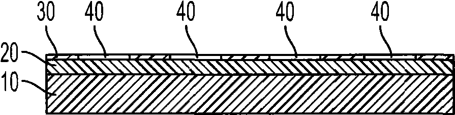
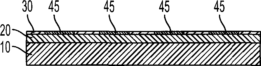
[0078] A nitride passivation layer is formed on the top surface of the silicon semiconductor substrate. Holes are formed in the nitride passivation layer using laser direct writing. Each of the plurality of holes has a diameter of about 20 μm and a pitch of about 0.25 mm. A Ni conductive contact layer is deposited on the nitride passivation layer and within the plurality of holes formed in the nitride passivation layer. The thickness of the Ni contact layer is about 100 nm.

[0079] An Ag paste is deposited via screen printing on the Ni conductive contact layer in alignment or registration with the plurality of holes formed in the nitride passivation layer. Next, the silicon substrate was fired at about 500° C. to form an Ag / Ni multilayer electrode structure with sintered current-carrying Ag gridlines.

[0080] The contact resistance of the Ag / Ni multilayer electrode was about less than 0.03 ohms for a wire about 25.4 mm long. In addition, the contact resistance of the Ag / ...


PUM


Abstract

Methods for forming a photovoltaic cell electrode structure, wherein the photovoltaic cell includes a semiconductor substrate having a passivation layer thereon, includes providing a plurality of contact openings through the passivation layer to the semiconductor substrate, selectively plating a contact metal into the plurality of contact openings to deposit the contact metal, depositing a metal containing material on the deposited contact metal, and firing the deposited contact metal and the deposited metal containing material. The metal containing material may include a paste containing a silver or silver alloy along with a glass frit and is substantially free to completely free of lead. The methods may also use light activation of the passivation layer or use seed layers to assist in the plating.

Description

technical field [0001] Described in this specification is a method of forming the multilayer electrode structure of a silicon photovoltaic cell, ie, a silicon solar cell. These methods provide silicon solar cells with low contact resistance and small contact area, thus providing improved contact resistivity over electrode structures formed with glass frit. These methods also result in less environmental distress than using lead-based frits, a notable improvement since solar energy is a so-called "clean" energy source. Background technique [0002] A solar cell is a typical photovoltaic device that converts sunlight directly into electricity. Solar cells generally comprise a silicon semiconductor that absorbs light radiation, such as sunlight, in a manner that generates free electrons, which then flow in a built-in field to generate direct current (hereinafter "DC") electricity. DC power generated by several photovoltaic (PV) cells can be harvested onto grids associated wit...

Claims


Application Information

Patent Timeline
IPC IPC(8): H01L31/18
CPCH01L31/18H01L31/022425Y02E10/50
Inventor B·徐K·A·里涛D·K·福克
Owner PALO ALTO RES CENT INC
Why Eureka
Try Eureka