

Method for packaging light emitting diode
A technology for light-emitting diodes and packaging methods, which is applied to semiconductor devices, electrical components, circuits, etc., and can solve problems such as inability to respond to design changes quickly, delaying production schedules, and deformation.
- Summary
- Abstract
- Description
- Claims
- Application Information
AI Technical Summary
Problems solved by technology
Method used
Image

Examples
Embodiment Construction
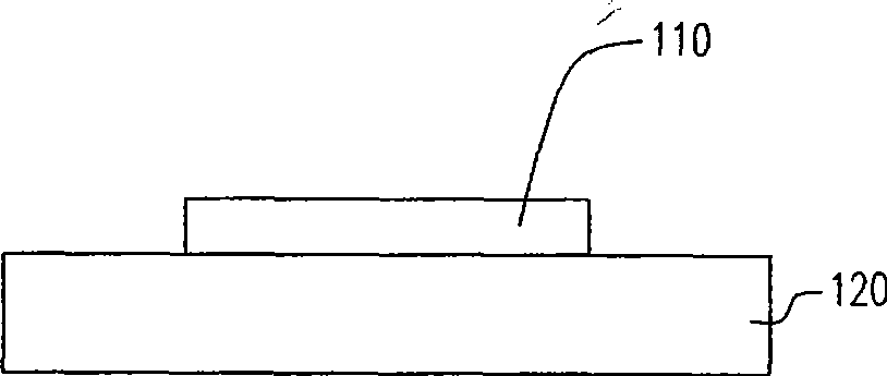
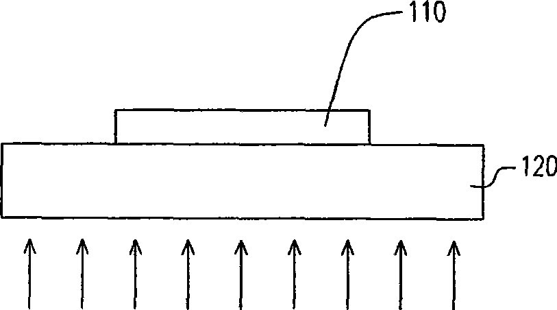
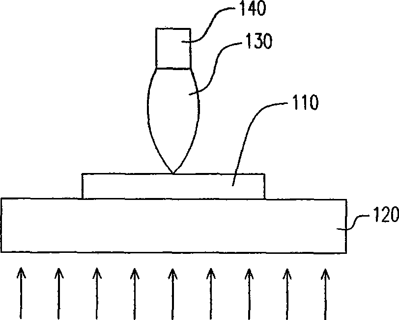
[0025] Figure 1A ~ Figure 1E It is a schematic cross-sectional view of a light emitting diode packaging method according to an embodiment of the present invention. Please refer to Figure 1A Firstly, a light emitting diode chip 110 is bonded to a carrier 120 so that the light emitting diode chip 110 is electrically connected to the carrier 120 . The aforementioned carrier 120 generally refers to any carrier board capable of carrying the LED chip 110 and electrically connected to the LED chip 110 . In this embodiment, the carrier 120 may be a printed circuit board (Printed Circuit Board, PCB), and the printed circuit board is made of ceramic material or plastic material, for example. In addition, the printed circuit board can also be a metal core printed circuit board (Metal Core Printed Circuit Board, MCPCB) or a flexible printed circuit board (Flexible Printed Circuit) with good heat dissipation properties. In other words, the light-emitting diode 100 in this embodiment is...
PUM
| Property | Measurement | Unit |
|---|---|---|
| Viscosity | aaaaa | aaaaa |
Abstract
Description
Claims
Application Information