

Imprint method
a technology of imprinting and printing, applied in the field of imprinting methods, can solve problems such as pattern defects due to remaining particles
- Summary
- Abstract
- Description
- Claims
- Application Information
AI Technical Summary
Benefits of technology
Problems solved by technology
Method used
Image

Examples
first embodiment
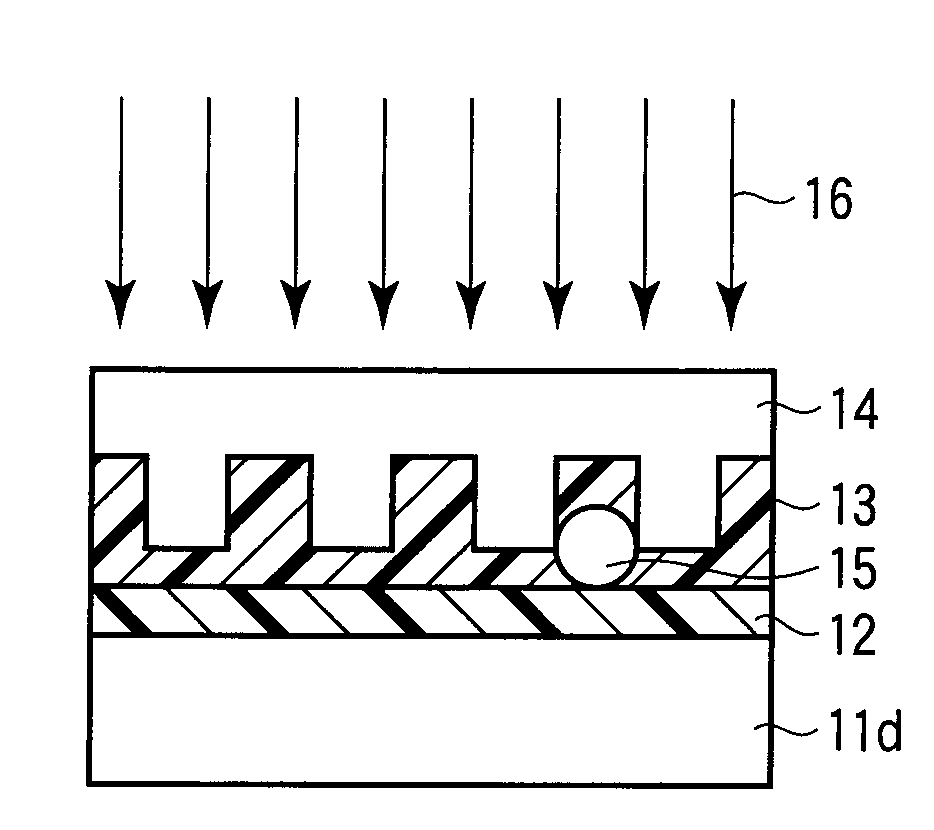
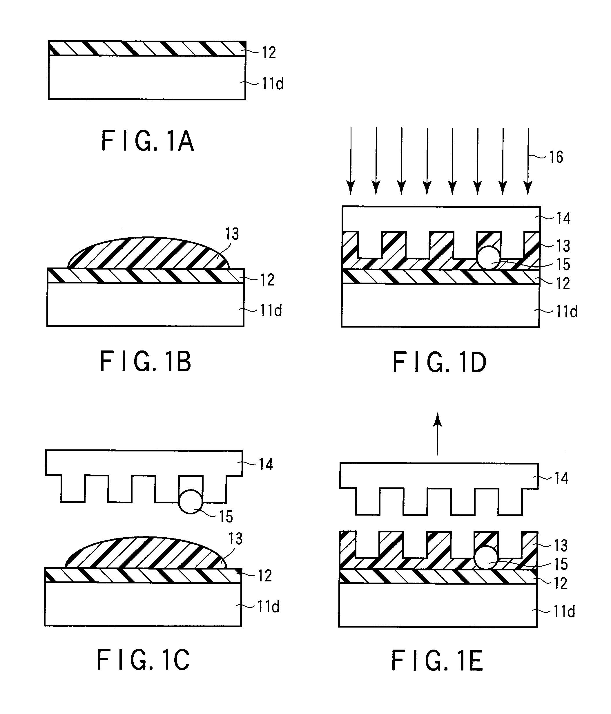
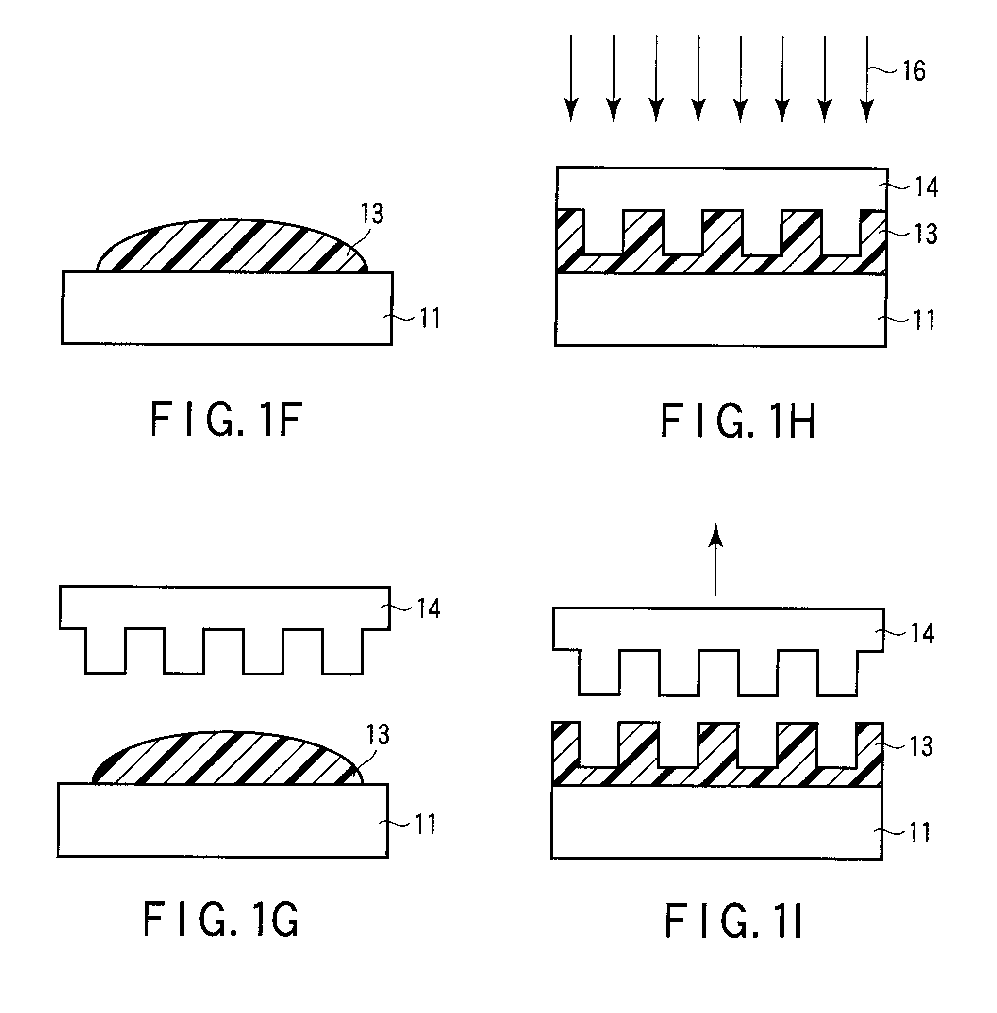
[0039]FIGS. 1A to 1I are cross-sectional views to explain an imprint method according to a first embodiment.
[0040]When a repeat defect (common defect) is detected during an imprinting onto a substrate on which a pattern is to be transferred, the substrate is unloaded from an imprint apparatus, and a dummy substrate is loaded in the imprint apparatus.
[0041]Here, the repeat defect is formed in a manner that a pattern defect shown in FIG. 18A is generated repeatedly at least two times, or a pattern defect shown in FIG. 18B is generating after the generation of the pattern defect shown in FIG. 18A. The repeat defect (common defect) is detected by a known defect inspection method.
[0042]In addition, the substrate is, for example, a silica substrate (transparent substrate), a silicon substrate (semiconductor substrate) and an SOI substrate (semiconductor substrate). The substrate may have a multi-layer structure. For example, the substrate (having a multi-layer structure) may comprise the ...
second embodiment
[0060]FIGS. 2A to 2D are cross-sectional views to explain an imprint method according to a second embodiment. In the following drawings, the same numerals are used to designate portions corresponding to the already given drawings, and the details are omitted.
[0061]When a repeat defect is detected during imprinting onto a substrate on which a pattern is to be transferred, a dummy substrate is prepared which comprises an Si wafer 11d and a light curable resin 13d coated (shot) on the Si wafer 11d as shown in FIG. 2A.
[0062]The light curable resin 13d has high adhesiveness to a template compared with a surface of a substrate used for a normal imprint recipe. In the present embodiment, a light curable resin having higher shrinkage ratio and higher mechanical strength after the hardening than a light curable resin used for a normal imprint recipe (surface of the substrate) is used as the light curable resin 13d.
[0063]Next, as shown in FIG. 2B, the substrate 11d and the template 14 are al...
third embodiment
[0068]FIG. 3 is a view schematically showing an imprint apparatus according to a third embodiment.
[0069]The imprint apparatus of the present embodiment comprises a stage 21 on which the substrate 11 is to be placed, a template holding assembly 22 provided above the stage 21 and configured to hold the template 14 including a pattern formed of concave and convex (transfer pattern), a vacuum device 23 configured to maintain a vacuum state between the template 14 and the substrate 11, and control device 24 configured to control each units 21, 22, and 23.
[0070]The vacuum device 23 comprises an exhaust pipe 25 and a vacuum pump 26 connected to the exhaust pipe 25. As shown in FIG. 4, the exhaust pipe 25 includes a first exhaust pipe 251 and a second exhaust pipe 252. A suction port 271 of the first exhaust pipe 251 is positioned on a side of the template 14, a suction port 272 of the second exhaust pipe 252 is positioned on an outside of template 14. The first exhaust pipe 251 is configur...
PUM
| Property | Measurement | Unit |
|---|---|---|
| thickness | aaaaa | aaaaa |
| thickness | aaaaa | aaaaa |
| thickness | aaaaa | aaaaa |
Abstract
Description
Claims
Application Information