A semiconductor material property measurement device and method based on double probe beam

A technology for material properties and measuring devices, applied in color/spectral properties measurement, measuring devices, material analysis by optical means, etc.

Inactive Publication Date: 2009-10-07
INST OF OPTICS & ELECTRONICS - CHINESE ACAD OF SCI
View PDF1 Cites 17 Cited by
  • Summary
  • Abstract
  • Description
  • Claims
  • Application Information

AI Technical Summary

Problems solved by technology

Sometimes it is necessary to use these two independent measurement methods to measure the characteristic parameters of semiconductor materials at the same time in the application. If the meas...

Method used


Image

  • A semiconductor material property measurement device and method based on double probe beam
  • A semiconductor material property measurement device and method based on double probe beam
  • A semiconductor material property measurement device and method based on double probe beam

Examples


Embodiment Construction

[0037] Embodiments of the present invention can be more fully understood from the following detailed description, which should be read in conjunction with the accompanying drawings. However, it should be noted that the specific embodiment only provides a description of the measurement of some semiconductor material characteristic parameters, but the present invention is not limited to this specific embodiment, and various Variety.

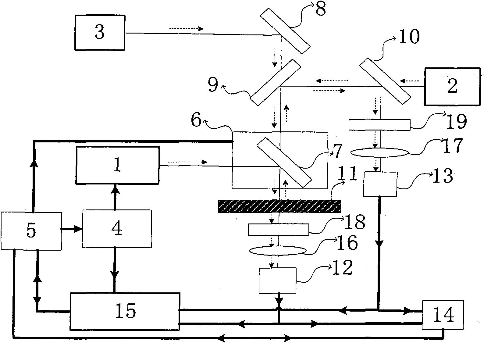
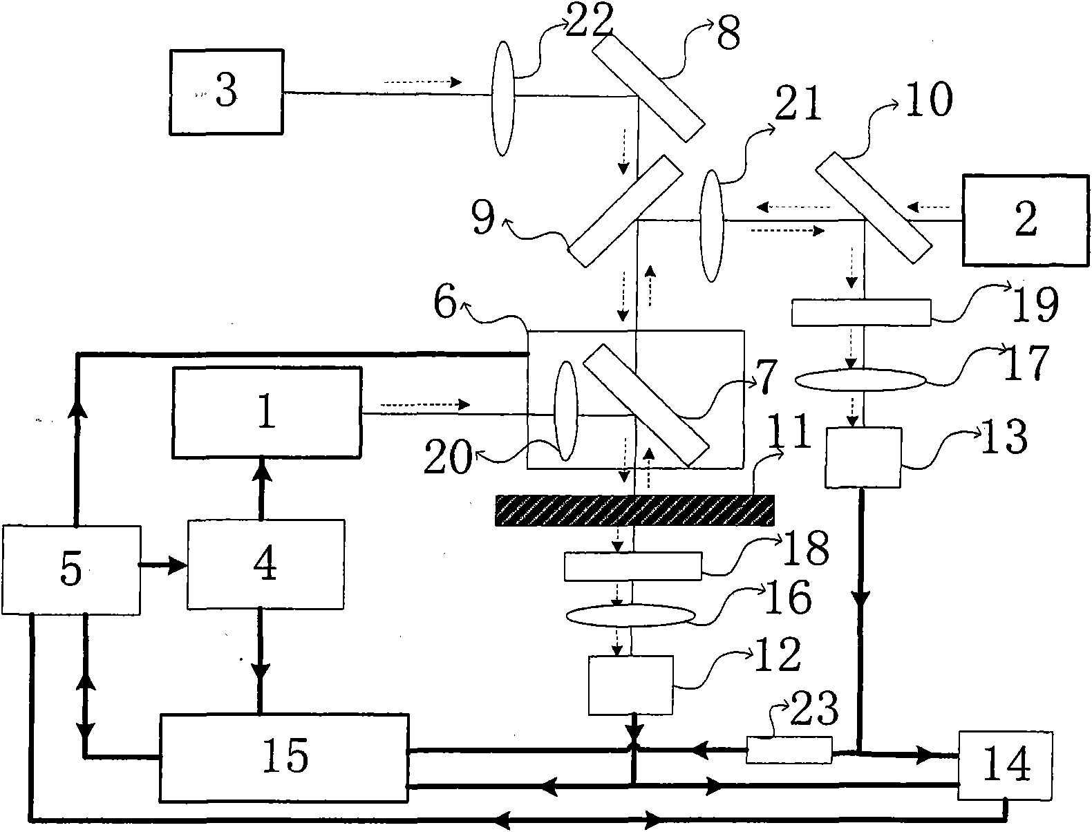
[0038] Firstly, a kind of semiconductor material characteristic measurement device based on double detection beams provided by the present invention is introduced. The device is as attached figure 1 As shown, it includes an excitation light source 1 for generating excitation light; a detection light source 2 for generating light modulation reflection signal detection light; a detection light source 3 for generating free carrier absorption signal detection light; an excitation light modulation system 4 for modulating the intensity of excitation ligh...


PUM


Abstract

The invention is a semiconductor material property measurement device and method based on double probe beam for measuring the characteristic parameters of semiconductor materials and monitoring the doping process. It obtains the free carrier absorption signal and the light-modulated reflecting signal simultaneously in the same set of test system based on the absorption of the exciting light of the periodic intensity modulation by the semiconductor materials; it obtains the free carrier absorption signal and light-modulated reflecting signal of the frequency domain by changing the modulation frequency of the exciting light; it obtains the free carrier absorption signal and light-modulated reflecting signal of the spatial domain by changing the spacing between the exciting light and the probe light; it may obtain the characteristic parameters of semiconductor materials and the process parameters as the doping concentration through the analysis and processing of the signals obtained or the comparison with the signal data of the calibration sample. The invention makes up for the shortcomings of the single technology and improves the measurement accuracy; it obtains two kinds of signals simultaneously in one device and more important parameters of the semiconductor materials comparing with the single technology.

Description

technical field [0001] The invention belongs to the technical field of non-destructive testing of semiconductor materials, and in particular relates to a measuring device and a measuring method for determining semiconductor material characteristics by combining free carrier absorption technology and light modulation reflection technology, that is, double detection beam detection technology. Background technique [0002] Only by doping the semiconductor material to change its structure and resistivity, the semiconductor material can become a useful functional material. The precise monitoring of the impurity concentration doped in the semiconductor material and the processing technology such as annealing determines the performance of the semiconductor device to a large extent. In the monitoring process, some characteristic parameters of semiconductor materials are measured to judge whether the material processing is up to standard. Now that the size of semiconductor wafers is...

Claims


Application Information

Patent Timeline
IPC IPC(8): G01N21/31G01N21/17G01N21/88G01R27/02
Inventor 李斌成黄秋萍刘显明韩艳玲
Owner INST OF OPTICS & ELECTRONICS - CHINESE ACAD OF SCI
Why Eureka
Try Eureka