Chip data compressing and testing multiplex circuit and chip test circuit

A data compression and multiplexing technology, applied in the direction of electronic circuit testing, etc., can solve the problems of increased chip testing costs and production costs, and achieve the effects of improving test efficiency, increasing output, and reducing production costs

Active Publication Date: 2009-10-07
ETRON TECH INC
View PDF0 Cites 13 Cited by
  • Summary
  • Abstract
  • Description
  • Claims
  • Application Information

AI Technical Summary

Problems solved by technology

In this way, the number of test pins will increase, which will increase the cost of chip testing, and if the test rate of

Method used


Image

  • Chip data compressing and testing multiplex circuit and chip test circuit
  • Chip data compressing and testing multiplex circuit and chip test circuit
  • Chip data compressing and testing multiplex circuit and chip test circuit

Examples


Example Embodiment

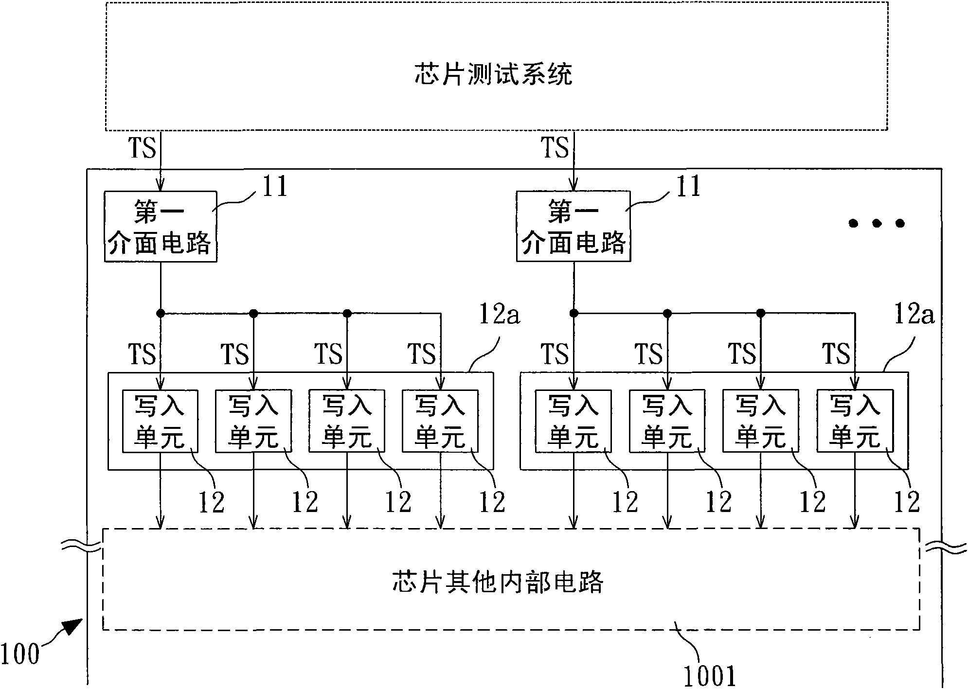
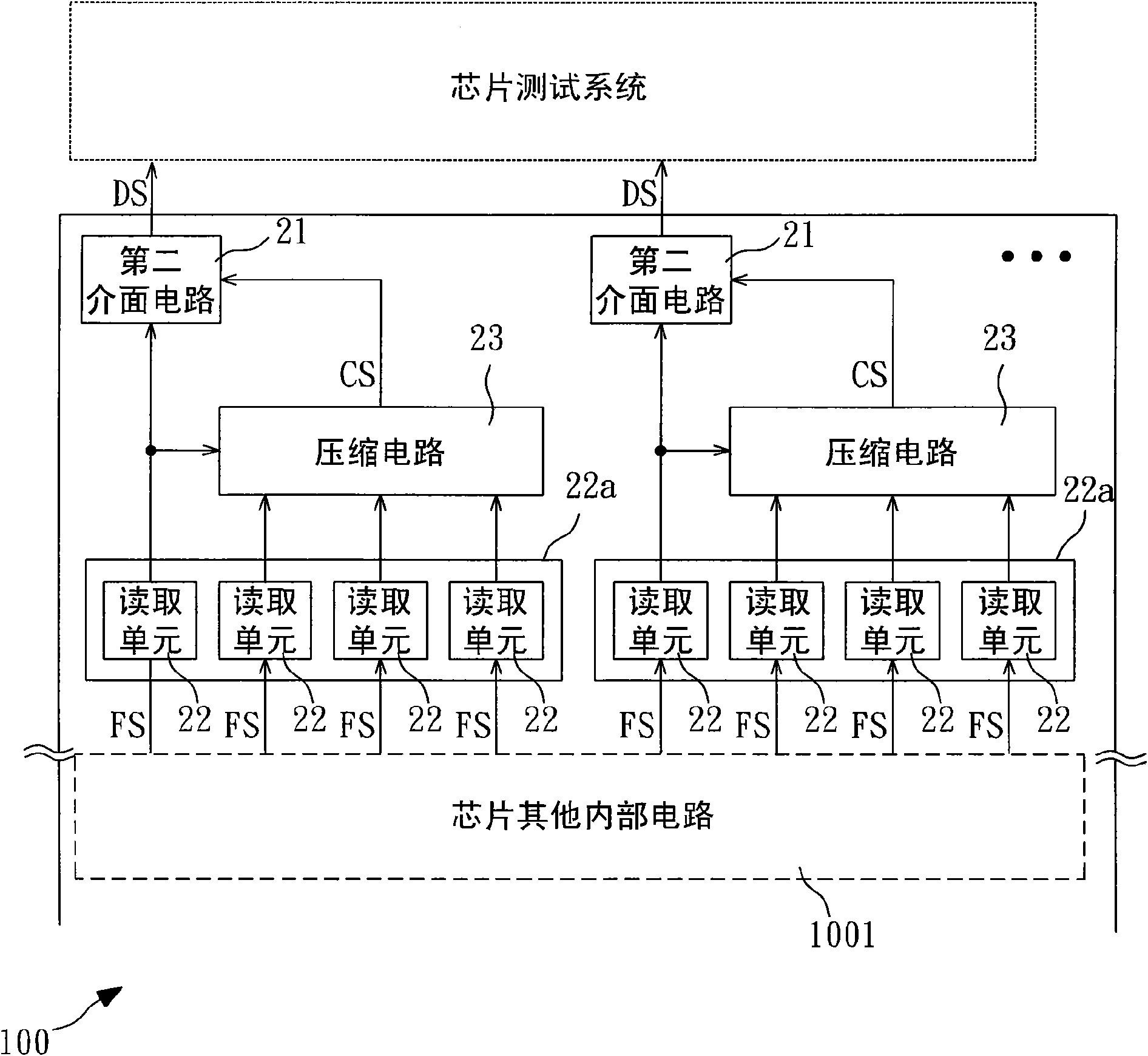
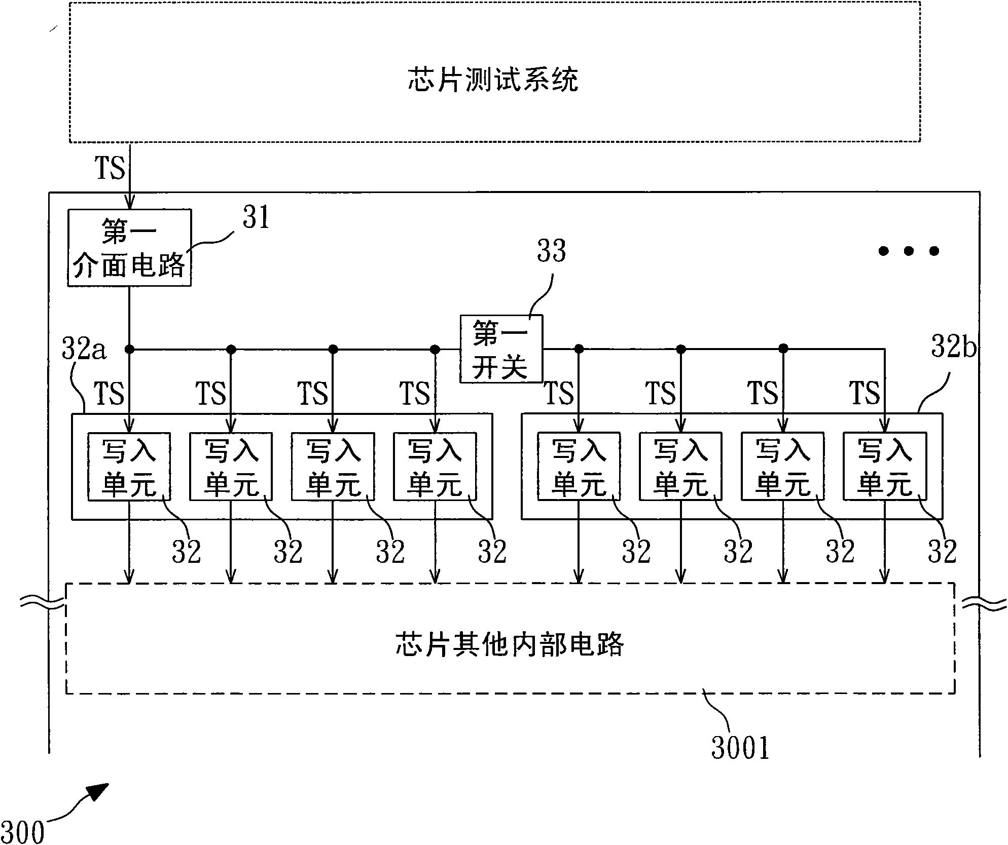
[0033] The chip data compression test multiplexing circuit (chip test circuit) of the present invention will be described in detail below with reference to the accompanying drawings, and the same components will be marked with the same symbols.

[0034] Figure 2A , Figure 2B A schematic diagram of a chip data compression test multiplexing circuit (chip test circuit) according to an embodiment of the present invention is shown. The chip data compression test multiplexing circuit 300 of an embodiment of the present invention includes a write circuit part (such as a Write) circuit that inputs a test signal TS to other internal circuits 3001 of the chip. Figure 2A Shown), and the feedback signal FS read circuit part (Read) obtained from other internal circuits 3001 of the chip (such as Figure 2B Shown).

[0035] Such asFigure 2A As shown, the writing circuit of the chip data compression test multiplexing circuit 300 according to an embodiment of the present invention includes a ...


PUM


Abstract

The invention discloses a chip data compressing and testing multiplex circuit, wherein a interface circuit can be switched between output units of different compression groups by a multiplexor, multiple groups of compressing and test data can be obtained by utilizing a single interface circuit, thereby effectively raising test speed.

Description

technical field [0001] The invention relates to a chip data compression test multiplexing circuit, in particular to a chip data compression test multiplexing circuit for improving the test output rate. Background technique [0002] An integrated circuit (Integrated Circuit, IC) is small in size and powerful in function, and is one of the indispensable electronic components of information equipment. In order to ensure the normal function of the chip, the chip must be strictly tested before leaving the factory. A simple test method is to input a known test signal to the circuit in the chip, and then obtain a feedback signal from the chip circuit, thereby judging whether the function of the chip is normal. [0003] Figure 1A A schematic diagram of a write portion of a known chip testing circuit 100 is shown. The writing part of the chip testing circuit 100 is connected with a chip testing system (such as a probe card) through the first interface circuit 11 , receives the tes...

Claims


Application Information

Patent Timeline
IPC IPC(8): G01R31/28
Inventor 袁德铭梁明正李国华
Owner ETRON TECH INC
Why Eureka
Try Eureka