Image display device and driving method of image display device

一种图像显示装置、驱动电路的技术,应用在静态指示器、仪器等方向,能够解决难以简化结构、图像质量恶化、难以正确地表现色阶等问题,达到高精度栅极电压的效果

Active Publication Date: 2009-10-14
JAPAN DISPLAY DESIGN & DEV CONTRACT CO LTD
View PDF2 Cites 14 Cited by
  • Summary
  • Abstract
  • Description
  • Claims
  • Application Information

AI Technical Summary

Problems solved by technology

[0055] Therefore, by Figure 25 When the signal line driving circuit 13 drives three signal lines in a time-division manner, if the number of lines of the display unit increases due to high definition, it will be difficult to set the gate voltage Vg of the driving transistor Tr3 to a color level with high precision. Problems with setting voltages VsigR, VsigG, and VsigB
In addition, when the terminal voltage of the storage capacitor Cs cannot be set to the gradation setting voltages VsigR, VsigG, and VsigB with high precision, it is difficult to express the gradation accurately, which causes image quality to deteriorate.
[0056] Also, when the resolution is low and the number of signal lines driven by the time-division method increases, it is also difficult to set the gate voltage Vg of the drive transistor Tr3 to the gradation setting voltages VsigR, VsigG with high accuracy. , VsigB
Therefore, at this time, it is difficult to reduce the number of terminals of the data driver, and it is difficult to simplify the structure

Method used


Image

  • Image display device and driving method of image display device
  • Image display device and driving method of image display device
  • Image display device and driving method of image display device

Examples


Embodiment 1

[0094] (1) Structure of Embodiment 1

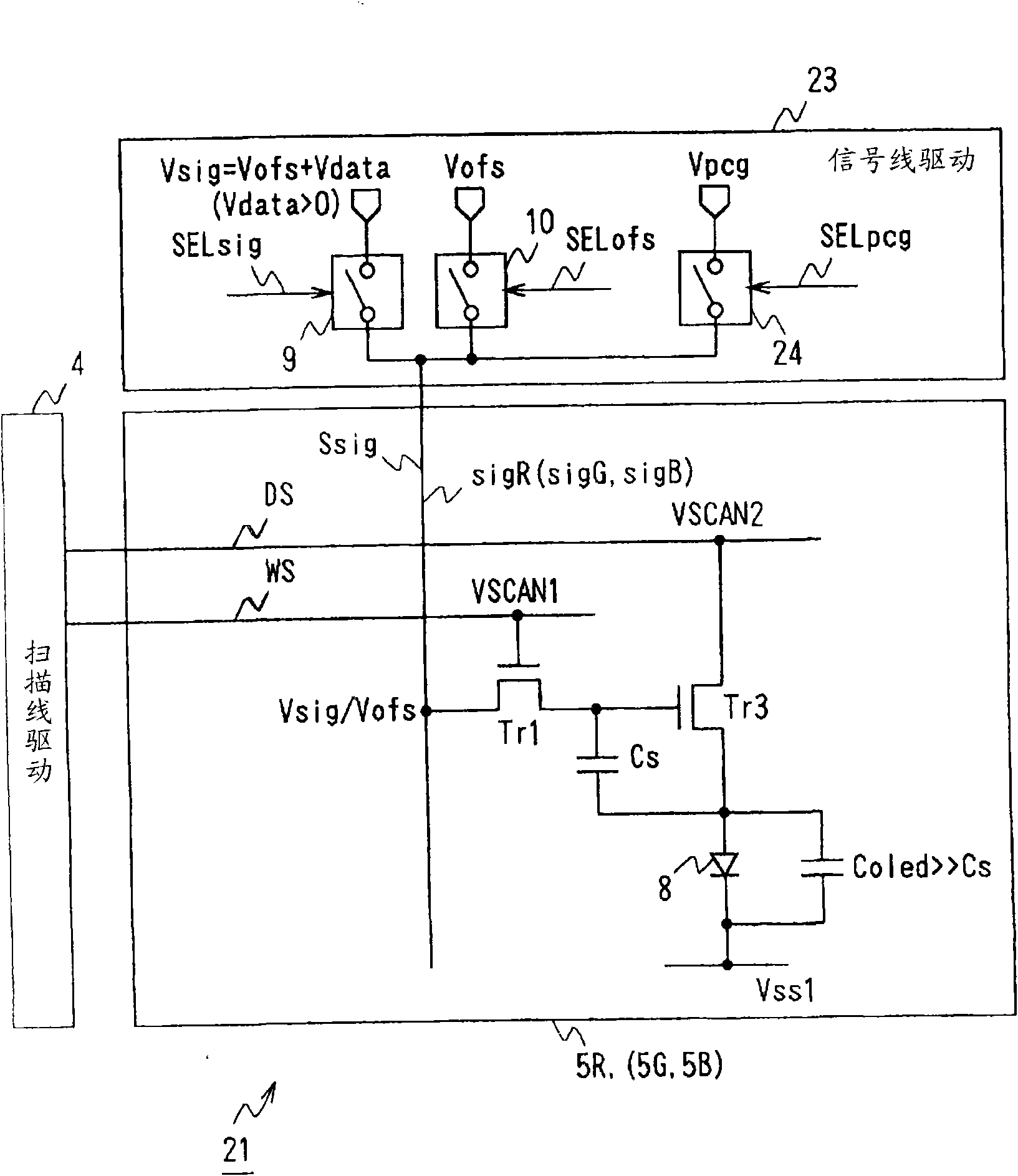
[0095] figure 1 is through with Figure 23 A diagram showing the image display device of Example 1 of the present invention for comparison. The image display device 21 of this embodiment is configured in the same manner as the image display device 1 described above except that the signal line drive circuit 23 is provided instead of the signal line drive circuit 3 .

[0096] Among them, the signal line drive circuit 23 is configured to selectively output the voltage Vsig for tone level setting, the fixed voltage Vofs for threshold voltage correction, and the precharge voltage Vpcg to the signal line sig via the switch circuits 9, 10, and 24, respectively. . Among them, the precharge voltage Vpcg is a voltage for raising the potential of the signal line sig in advance before setting the gate voltage Vg of the drive transistor Tr3 to the gradation setting voltage Vsig. The precharge voltage Vpcg is set to a voltage between the maximum v...

Embodiment 2

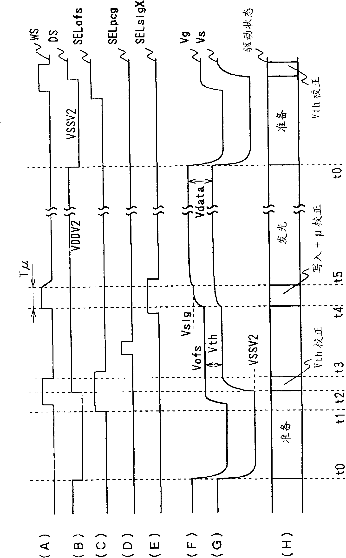
[0123] Figure 5 is through with figure 1 A diagram showing the image display device 31 of Example 2 of the present invention for comparison. also, Figure 6 is through with figure 2 A timing chart for explaining the operation of the pixel circuit in the image display device 31 is compared with the above. The image display device of this embodiment is applicable to the figure 1 Except for the signal line driving circuit 33 shown in , it has the same configuration as the image display device 21 of the first embodiment.

[0124] The signal line drive circuit 33 time-division-multiplexes the fixed voltage Vofs and the precharge voltage Vpcg to input it to the switch circuit 10 . The switch circuit 10 is controlled to be on and off by a calculation signal SELofs / pcg of a control signal SELofs for controlling the output of the fixed voltage Vofs and a control signal SELpcg for controlling the output of the precharge voltage Vpcg. In this embodiment, the output signal of th...

Embodiment 3

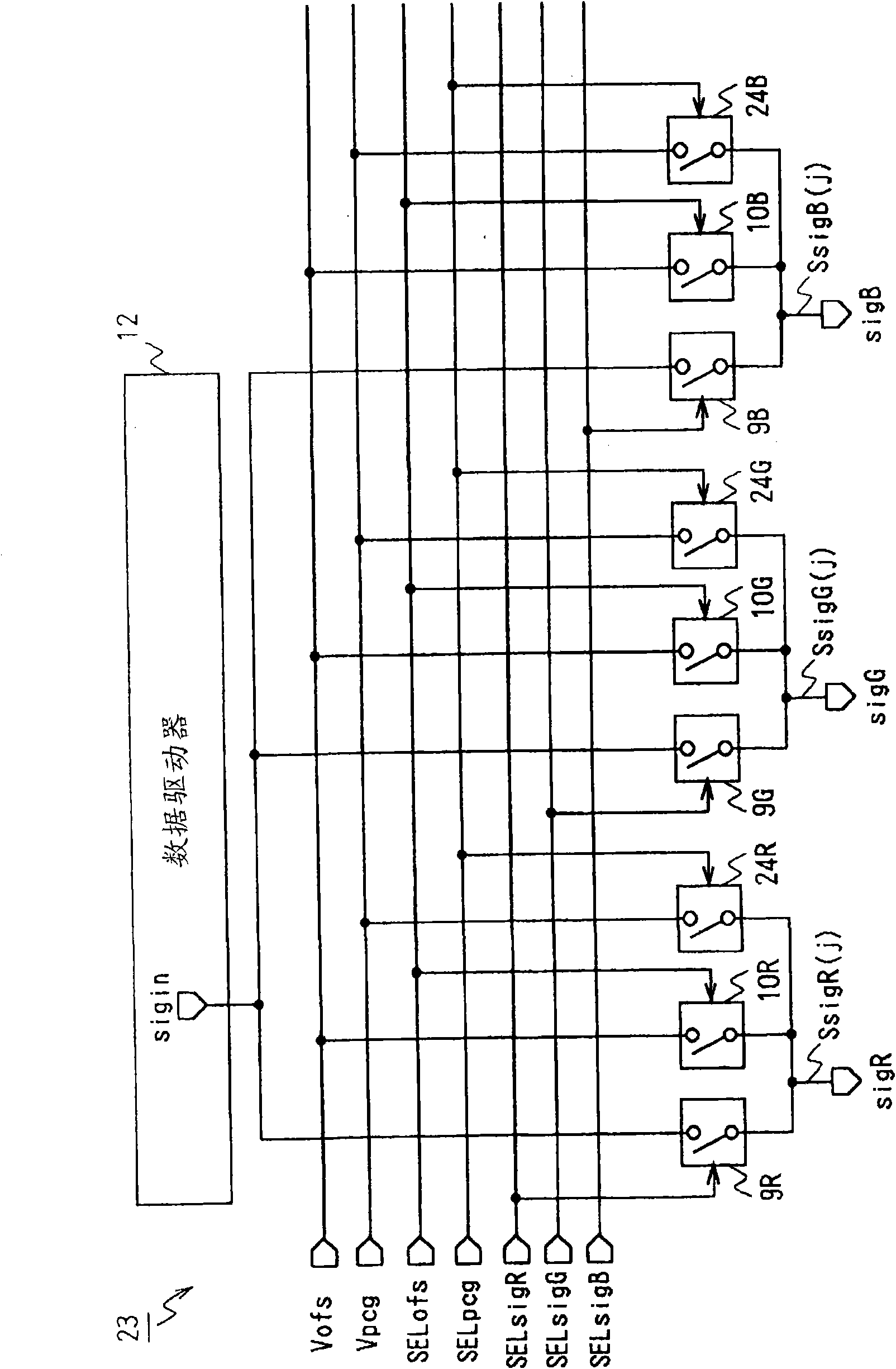
[0129] Figure 9 is through with image 3 A diagram showing a signal line driving circuit applied to the image display device according to Embodiment 3 of the present invention is shown in comparison with the drawings. The image display device of this embodiment is configured in the same manner as the image display device 21 of the first embodiment described above, except for the configuration of the signal line drive circuit 43 .

[0130] In this signal line drive circuit 43 , setting of the voltage Vsig for tone scale setting is performed in a time-divisional manner on a plurality of signal lines sig. In the image display device of this embodiment, in the process of raising the potential of the signal line sig to the precharge voltage Vpcg, corresponding to the time-divisional setting of the voltage Vsig for gradation setting, these multiple signals Line sig is executed in a time-division manner. The signal line drive circuit 43 has the same configuration as the signal li...


PUM


Abstract

The present invention relates to an image display device in which a self-luminescent component is driven through a driving transistor. Namely the grid voltage of driving transistor can be set with a high precision in a state that a plurality of signal lines are executed with time-division driving. According to the invention, before executing the time-division driving to the plurality of signal lines (sig) for setting the color gradation of each pixel circuit, at least the electric potential of the signal line (sig) is set to a precharging electric voltage (Vpcg).

Description

technical field [0001] The present invention relates to an image display device and a method for driving the image display device, and is applicable to, for example, an active matrix type image display device composed of organic EL (Electro Luminescence) elements. The present invention relates to an image display device that drives a self-emitting element by driving a transistor by setting at least the potential of a signal line to a precharge voltage in advance. Even when driving a plurality of signal lines in a time-division manner, it is possible to set the potential with high precision. Determine the gate voltage of the drive transistor. Background technique [0002] Conventionally, in an active matrix image display device using organic EL elements, pixel circuits including organic EL elements and drive circuits for driving the organic EL elements are arranged in a matrix to form a display unit. Such an image display device displays a desired image by driving each pixel...

Claims


Application Information

Patent Timeline
Patent Type & Authority Applications(China)
IPC IPC(8): G09G3/32G09G3/20
CPCG09G2300/0814G09G2320/043G09G3/325G09G3/3233G09G2300/0819G09G3/3291G09G2300/0852
Inventor 浅野慎
Owner JAPAN DISPLAY DESIGN & DEV CONTRACT CO LTD
Why Eureka
Try Eureka