Method and device for non-contact detection of LED luminescence properties

A technology of luminous characteristics and detection methods, applied in non-contact testing, testing optical performance, testing of single semiconductor devices, etc., can solve the problem of no detection method, and achieve the effect of avoiding contact damage and reducing costs

Inactive Publication Date: 2009-10-21
CHONGQING UNIV
View PDF5 Cites 19 Cited by
  • Summary
  • Abstract
  • Description
  • Claims
  • Application Information

AI Technical Summary

Problems solved by technology

However, there is no ideal detectio

Method used


Image

  • Method and device for non-contact detection of LED luminescence properties

Examples


Embodiment Construction

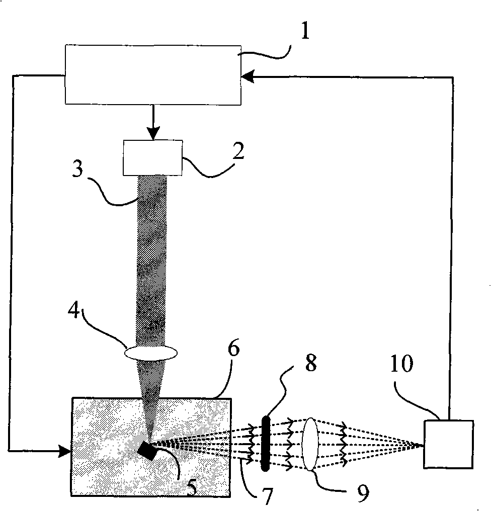
[0016] Rationale: Luminescence is the process by which an object converts energy absorbed in some way into light radiation. LED is a typical semiconductor light-emitting device. Its light-emitting mechanism is the recombination of non-equilibrium carriers. The light-emitting process of LED includes three parts: carrier injection, radiative recombination and light energy transmission. There are generally two ways to inject carriers: current injection and light absorption. The luminescence caused by current injection is called electroluminescence. This is the general luminescence method used by LEDs as devices. Therefore, it is usually necessary to test the luminescence characteristics of LEDs, which are measured by applying ohmic contact with chips or finished products and applying electric injection. Luminescence caused by light absorption is called photoluminescence. From the light-emitting process of LED, it can be seen that only the carrier injection method of electrolumin...


PUM


Abstract

The invention discloses a non-contact detection method of LED luminescence properties. The method comprises the following steps: a PN junction area for an LED device to be tested is irradiated with short-term pulsed light at the constant temperature, and the detection to the luminescence properties of the LED device to be tested is realized by detecting the self-luminescent spectrum of a PN junction; the invention also discloses a non-contact detection device based on the LED luminescence properties of the method; and the invention has the beneficial effects that the luminescence properties of the epitaxial wafer of the LED, the wafer or the single LED chip can be detected under the condition that the device to be tested is not contacted, therefore, the contact damage of the LED device to be tested is avoided, the detection and the screening of the LED products are propelled to the chip even to the epitaxial wafer link from the link of the finished products, and the cost of the LED is reduced.

Description

technical field [0001] The invention relates to the technical field of chip detection, and more specifically relates to a non-contact detection method and device for LED luminous characteristics. technical background [0002] LED (Light Emitting Diode) is widely used in indicator lights, signal lights, display screens, landscape lighting and other fields due to its inherent characteristics, such as power saving, long life, vibration resistance, fast response speed, and cold light source. However, due to the lack of ideal testing equipment, testing and sorting has become a technical bottleneck for many LED chip manufacturers in improving production efficiency and reducing production costs. Therefore, it is of great significance for the development of the LED chip industry to propose a fast, low-cost, and non-destructive testing method and equipment for each LED chip unit on an epitaxial wafer or wafer. [0003] The US invention patent (patent number: US006670820B2) discloses...

Claims


Application Information

Patent Timeline
IPC IPC(8): G01R31/265G01M11/02
Inventor 李平文玉梅李恋文静
Owner CHONGQING UNIV
Why Eureka
Try Eureka