Electronic device manufacturing method and manufacturing device

A manufacturing method and technology of electronic devices, applied in semiconductor/solid-state device manufacturing, electric solid-state devices, electrical components, etc., can solve problems such as damage to components or joints, inability to ensure filling, insufficient fluidity, etc., to prevent joints Effects of destroying, shortening curing time, and improving immersion

Active Publication Date: 2012-02-01
MURATA MFG CO LTD
View PDF5 Cites 0 Cited by
  • Summary
  • Abstract
  • Description
  • Claims
  • Application Information

AI Technical Summary

Problems solved by technology

It is assumed that when using a resin material that deviates from this physical parameter, there is a problem that: it will cause damage to the mounted component or the joint; or due to high viscosity, the fluidity is not enough to ensure the required filling property

Method used


Image

  • Electronic device manufacturing method and manufacturing device
  • Electronic device manufacturing method and manufacturing device
  • Electronic device manufacturing method and manufacturing device

Examples


no. 1 approach 》

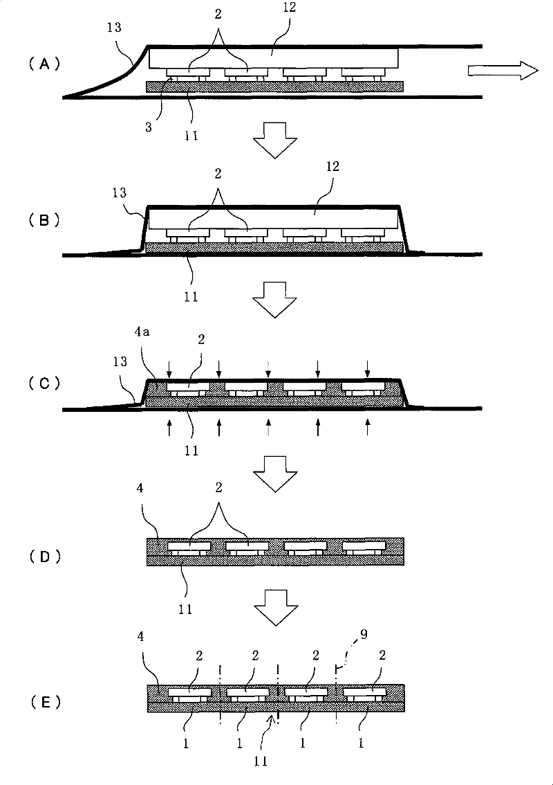
[0074] refer to Figure 2 ~ Figure 6 A method of manufacturing an electronic device and a manufacturing apparatus thereof according to the first embodiment of the present invention will be described.

[0075] figure 2 It is a sectional view showing the state in the sheet resin lamination step and the state in the resin filling and sealing step.

[0076] Each process will be described in detail later, but in the sheet resin lamination process, such as figure 2 As shown in (A), the sheet resin 24 is laminated on the mounting substrate 23 corresponding to the "mounting assembly substrate" according to the present invention, sandwiched between the spacers 22 and 25, and these laminates are further placed on the substrate. The upper part of the bottom plate 21 is placed in a gas barrier bag (hereinafter referred to as "package") 30 to constitute a package 50 containing a substrate.

[0077] figure 2 (B) is a partially enlarged cross-sectional view showing a mounting state of...

no. 2 approach 》

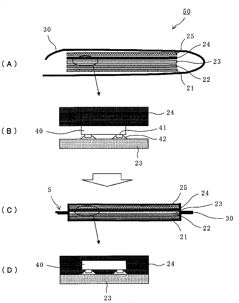
[0111] refer to Figure 7 ~ Figure 9 A method of manufacturing an electronic device and a manufacturing apparatus thereof according to a second embodiment of the present invention will be described.

[0112] Figure 7 , Figure 8 Each process of the manufacturing method of an electronic device is shown with a figure. Figure 7 (A) and (B) are sectional views showing the state in the sheet resin lamination step, Figure 7 (C) is a cross-sectional view showing the state in the solvent volatilization step. in addition, Figure 7 (D) is the first half step of the resin filling and sealing step.

[0113] In the second embodiment, an electronic device on which a relatively large chip-shaped electronic functional element is mounted is targeted.

[0114] First, in the sheet resin lamination process, such as Figure 7 As shown in (A), for example, a sheet resin 24 is laminated on a mounting substrate (mounting aggregate substrate) 23 on which a large chip-shaped electronic funct...

no. 3 approach 》

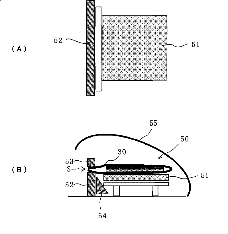
[0129] refer to Figure 10 A method of manufacturing an electronic device and a manufacturing apparatus thereof according to a third embodiment of the present invention will be described.

[0130] Figure 10 It is a diagram showing the state of heating and pressurizing the package containing the substrate in the resin filling and sealing process. In the second embodiment, the package 50 containing the substrate is heated and pressurized by the thermostatic hydrostatic pressure method. Figure 10 In the example shown, the package 50 containing the substrate is placed on the table 71 of the uniaxial press device, and the package 50 containing the substrate is pressed with a predetermined pressing force while being heated by the movable part 7 of the uniaxial press device. 50.

[0131] The package 50 with the substrate is composed of Figure 7 The steps shown in (A) to (D) have the same step configuration.

[0132] The heating temperature at the time of pressurization is a t...


PUM


Abstract

The present invention provides a method and an apparatus for manufacturing an electronic device, capable of obtaining a higher resin filling character even by using a sheet material resin with a large dissolvent volatilization amount, and restraining a damage to a junction of a mounted element without a gas generation. In a process of stacking the sheet material resin, a metallic bottom board (21) is stacked with a separator (22), a mounting substrate (23) and the sheet material resin (24) in sequence, a separator (25) is further stacked thereon, then the bottom board is loaded in a package (30) to form a package (50) having a substrate. After, in a dissolvent volatilization process, the package (50) having the substrate is placed on a heating table of a heating laminating device, then is decompressed and heated until less than a solidification temperature of the sheet material resin (24). Thereafter the dissolvent of the sheet material resin will be volatilized. In a resin filling and sealing process, the package (30) is sealed, a laminating package is sealed, a vacuum chamber is opened and returns to the atmosphere pressure. Then, the sheet material resin is heated under a condition of packaging to be solidified formally.

Description

technical field [0001] The present invention relates to a manufacturing method of an electronic device such as a chip-scale package and a manufacturing apparatus thereof. Background technique [0002] Conventionally, chip size packages (CSP, chip size packages) of various structures have been developed in order to realize miniaturization and thinning of packages including chip-shaped electronic functional elements such as semiconductor bare chips. [0003] Patent Document 1 discloses a technology for resin-sealed packaging for such a purpose. [0004] figure 1 It is each process drawing at the time of manufacture of the electronic device disclosed in patent document 1. [0005] First, in the installation process, such as figure 1 As shown in (A), the components are mounted on the mounting assembly substrate 11 through the protruding electrodes 3 ; in the placement process, the resin film 12 is placed on each component 2 . In the following vacuum packaging process, such a...

Claims


Application Information

Patent Timeline
Patent Type & Authority Patents(China)
IPC IPC(8): H01L21/50H01L21/58H01L21/56H01L21/78H01L21/00
CPCH01L2924/01015H01L2924/01023H01L2924/01065H01L2924/01082H01L2924/01079H01L2224/97H01L2924/01068H01L2924/12041H01L2924/09701H01L2224/16H01L24/97H01L2924/01005H01L2924/01033H01L2924/01006H01L2924/01073H01L2924/01075H01L2924/01013H01L2924/15787H01L2224/81H01L2924/00
Inventor 久米宗一胜部彰夫田中启
Owner MURATA MFG CO LTD
Why Eureka
Try Eureka