Density conversion method and density conversion device for PCB test machine

A density conversion and conversion device technology, which is applied in the direction of measuring devices, coupling devices, electronic circuit testing, etc., can solve problems such as enterprise failure, small solder joints, dense density, etc., to eliminate gaps, improve reliability, and ensure electrical connections Effect

Active Publication Date: 2013-04-10
SHENZHEN MASONE ELECTRONICS
View PDF0 Cites 0 Cited by
  • Summary
  • Abstract
  • Description
  • Claims
  • Application Information

AI Technical Summary

Problems solved by technology

[0002] In the PCB testing industry, there is a standard universal test point specification - four density (that is, 400 test contact points are evenly arranged in 1 square inch), and each test point must be connected to the same test circuit, while the existing PCB board test equipment is to directly solder the test circuit pins to the test contact points through the connection for testing. However, the integration of circuit boards is getting higher and higher, and the solder joints are getting smaller and denser. Compared with Under the circumstances, the development of PCB board testing machines often lags behind. In addition, the price of PCB board testing machines is very high, and the companies that use them often cannot afford to update the corresponding testing machines. Lost in the fierce market tide

Method used


Image

  • Density conversion method and density conversion device for PCB test machine
  • Density conversion method and density conversion device for PCB test machine
  • Density conversion method and density conversion device for PCB test machine

Examples


Embodiment Construction

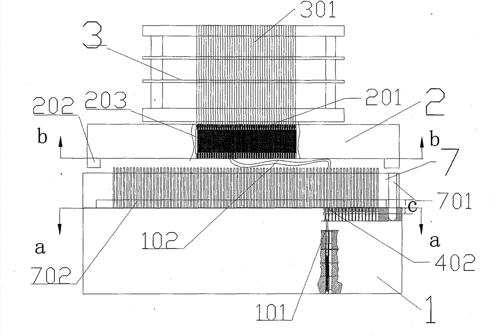
[0015] A density conversion device for a PCB testing machine, the conversion device is arranged between the needle bed 1 of the testing machine and the test fixture 3, and is used to convert the test fixture 3 with a higher probe density into the one with a lower probe density. On the needle bed 1 of the testing machine, the purpose of testing high-density PCB boards is realized.

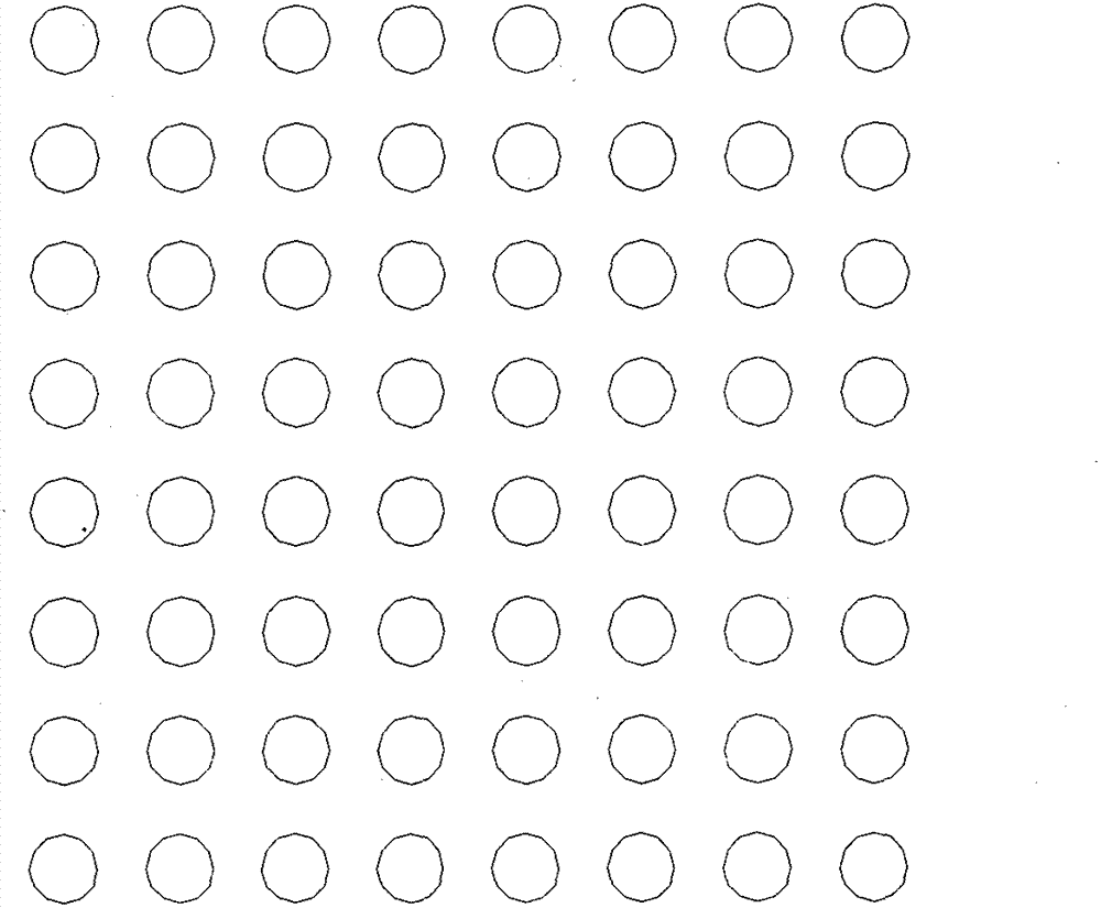
[0016] see figure 1 , the conversion device includes upper and lower layers, and the lower layer is a needle row substrate 7 arranged on the needle bed 1 of the testing machine, and the needle bed probes 101 of the testing machine are arranged in a lower four-density arrangement, see figure 2 The a-a cross-sectional view of the needle row substrate 7 is set corresponding to the needle bed probe 101 of the testing machine. In addition, the protruding length of the lower end of the connecting pin 702 is slightly longer than the distance c between the lower surface of the housing and the needle bed p...


PUM


Abstract

The invention relates to a density conversion device for a PCB test machine. The invention is characterized in that the conversion device comprises a conversion dial arranged at the upper layer and a winding wire arranged at the lower layer, wherein the conversion dial is provided with a spring return mechanism to ensure good electrical connection between a contact point and a probe of the test fixture, and thus, the gap between the contact point and the probe of the test fixture caused by mutual extrusion or relative position change can be eliminated in time by the self-reset function of the spring return mechanism; and one end of the winding wire arranged at the lower layer of the conversion device is connected with a lead wire of the conversion dial, and the other end is in contact with a probe of the test machine needle bed to enable a spring below the probe to be in a compressing state so as to ensure good electrical contact between the probe of the test machine needle bed and the lead wire. The conversion device greatly improves the reliability of test after density conversion by the cooperation of the conversion dial and the winding wire, therefore, the test for a high-density PCB without changing the original configuration of the test machine is feasible.

Description

【Technical field】 [0001] The invention relates to the field of printed circuit board (Printed Circuit Board; PCB) testing, in particular to a density conversion device for a PCB testing machine. 【Background technique】 [0002] In the PCB testing industry, there is a standard universal test point specification - four density (that is, 400 test contact points are evenly arranged in 1 square inch), and each test point must be connected to the same test circuit, while the existing PCB board test equipment is to directly solder the test circuit pins to the test contact points through the connection for testing. However, the integration of circuit boards is getting higher and higher, and the solder joints are getting smaller and denser. Compared with Under the circumstances, the development of PCB board testing machines often lags behind. In addition, the price of PCB board testing machines is very high, and the companies that use them often cannot afford to update the correspondi...

Claims


Application Information

Patent Timeline
Patent Type & Authority Patents(China)
IPC IPC(8): G01R1/02G01R1/073G01R31/28H01R31/06
Inventor 武勇潘海胡泉金
Owner SHENZHEN MASONE ELECTRONICS
Why Eureka
Try Eureka