Manufacturing process for touch-control panel
A manufacturing process and touch panel technology, which is applied in the field of touch panel manufacturing process, can solve the problems of low yield rate of touch panel, and achieve the effects of improving yield rate, accurate alignment, and easy and accurate position
- Summary
- Abstract
- Description
- Claims
- Application Information
AI Technical Summary
Problems solved by technology
Method used
Image

Examples
Embodiment Construction
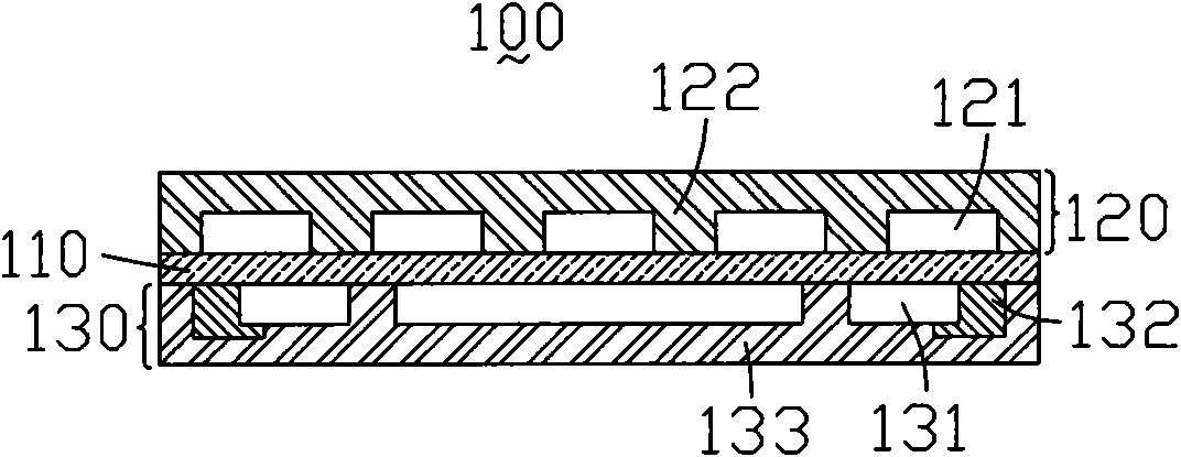
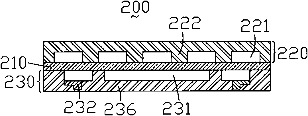
[0020] see figure 2 , is a structural schematic diagram of a touch panel. The touch panel 200 includes a substrate 210 , a sensing layer 220 formed on one side of the substrate 210 , and a driving layer 230 opposite to the sensing layer 220 disposed on the other side of the substrate 210 . The drive layer 230 includes a first transparent conductive pattern 231, two wires 232, a plurality of alignment marks 233 (refer to Figure 6 ) and the second protective layer 236 covering the first transparent conductive pattern 231 , the wire 232 and the alignment mark 233 . The first transparent conductive pattern 231 includes a plurality of driving electrode lines (not marked) parallel to each other and arranged at intervals on the substrate 210, the plurality of conductive lines 232 are electrically connected to the first transparent conductive pattern 231, the second protective layer 236 protects the first transparent conductive pattern 231 and the wire 232 .
[0021] The sensing ...
PUM
 Abstract
Description
Claims
Application Information
 - Generate Ideas
- Intellectual Property
- Life Sciences
- Materials
- Tech Scout
- Unparalleled Data Quality
- Higher Quality Content
- 60% Fewer Hallucinations
Browse by: Latest US Patents, China's latest patents, Technical Efficacy Thesaurus, Application Domain, Technology Topic, Popular Technical Reports.
© 2025 PatSnap. All rights reserved.Legal|Privacy policy|Modern Slavery Act Transparency Statement|Sitemap|About US| Contact US: help@patsnap.com