Method for detecting hot carrier effect of semiconductor device

A hot carrier and semiconductor technology is applied in the field of detecting the hot carrier effect of semiconductor devices, which can solve the problems of inaccurate estimation of the life of the device, affecting the accuracy of the device evaluation, etc., and achieve the effect of accurate detection results.

Inactive Publication Date: 2009-11-25
SEMICONDUCTOR MANUFACTURING INTERNATIONAL (BEIJING) CORP
View PDF1 Cites 9 Cited by
  • Summary
  • Abstract
  • Description
  • Claims
  • Application Information

AI Technical Summary

Problems solved by technology

[0010] The invention provides a method for detecting the hot carrier effect of a semiconductor device, which solves the problem of inaccurate estimation of device life in the prior art, thereby affecting the accuracy of device evaluation

Method used


Image

  • Method for detecting hot carrier effect of semiconductor device
  • Method for detecting hot carrier effect of semiconductor device
  • Method for detecting hot carrier effect of semiconductor device

Examples


Embodiment approach

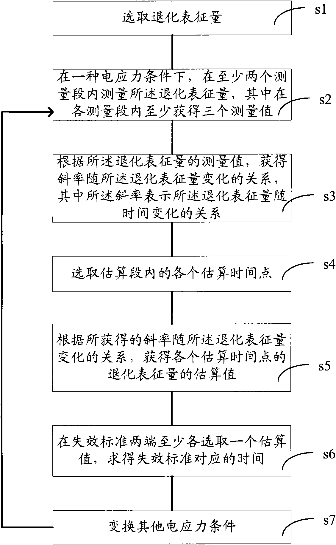
[0022] refer to figure 2 As shown, an embodiment of the method for detecting device lifetime of the present invention comprises:

[0023] Step s1, select the degraded characterization quantity;

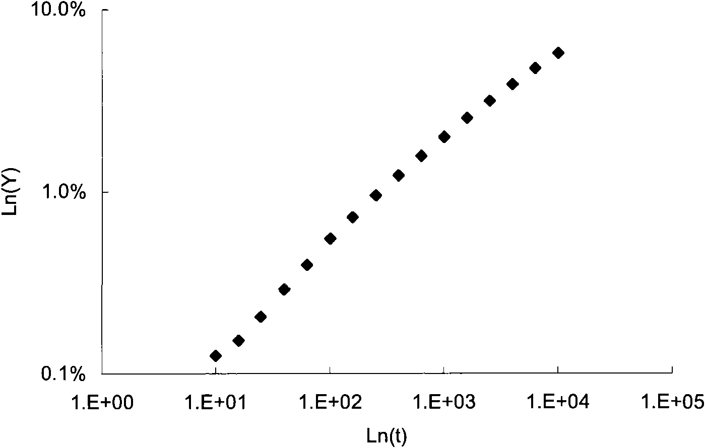
[0024] Step s2, under an electrical stress condition, measuring the degradation characterization quantity in at least two measurement intervals, wherein at least three measurement values ​​are obtained in each measurement interval;

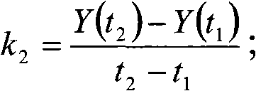
[0025] Step s3, according to the measured value of the degradation characterization, obtain the relationship between the slope and the change of the degradation characterization, wherein the slope represents the relationship of the degradation characterization with time;

[0026] Step s4, selecting each estimation time point in the estimation period;

[0027] Step s5, according to the obtained relationship between the slope and the change of the degradation characterization, obtain the estimated value of the degradation characterization at each estimat...


PUM


Abstract

The invention relates to a method for detecting hot carrier effect of a semiconductor device, which comprises the following steps: selecting degradation characterizing quantity; under the condition of various electric stress, measuring the degradation characterizing quantity in at least two measuring sections, wherein at least three measuring values are acquired in each measuring section; obtaining the relation of the slope changing along with the degradation characterizing quantity according to the measuring values of the degradation characterizing quantity, wherein the slope represents the relation of the degradation characterizing quantity changing along with the time; selecting various estimate time points in an estimate section; according to the obtained relation of slope changing along with the degradation characterizing quantity, acquiring estimate values of the degradation characterizing quantity of various estimate time points; and at least respectively selecting one estimate value at two ends of failure criteria to obtain the time corresponding to the failure criteria. The detecting result for estimating the service life of the device by the method is more accurate.

Description

technical field [0001] The invention relates to a method for detecting the hot carrier effect of a semiconductor device. Background technique [0002] At present, the silicon-silicon oxide interface state induced by hot carrier injection is the main manifestation of the hot carrier effect, and is also a key factor causing the degradation of other device parameters. Although the interface state density can be measured by charge pump technology, However, its distribution along the channel direction and in the energy space is difficult to accurately measure and simulate, and it is very difficult to use the interface state as a hot carrier degradation characterization. Therefore, electrical parameters that are sensitive to hot carrier effects, such as device drain current Ids, transconductance g m , threshold voltage V th The relative degradation amount ΔIds / Ids0, Δg m / g m 0, ΔV th / V th as a measure of hot-carrier degradation. At present, the commonly used method is to ...

Claims


Application Information

Patent Timeline
Patent Type & Authority Applications(China)
IPC IPC(8): G01R31/26
Inventor 郭强简维廷黄宏嘉
Owner SEMICONDUCTOR MANUFACTURING INTERNATIONAL (BEIJING) CORP
Why Eureka
Try Eureka