Wafer acceptance testing method, contact mat and probe card

A technology of wafer acceptance testing and contact pads, which is applied in the direction of electronic circuit testing, single semiconductor device testing, electrical measurement, etc., can solve the problem that the utilization rate of the wafer surface area cannot be improved, and achieve the effect of reducing the width and increasing the utilization rate

Inactive Publication Date: 2009-11-25
MPI CORP
View PDF1 Cites 14 Cited by
  • Summary
  • Abstract
  • Description
  • Claims
  • Application Information

AI Technical Summary

Problems solved by technology

Wafer surface area utilization cannot be improved due to dicing lanes occupying wafer surface area

Method used


Image

  • Wafer acceptance testing method, contact mat and probe card
  • Wafer acceptance testing method, contact mat and probe card
  • Wafer acceptance testing method, contact mat and probe card

Examples


Embodiment Construction

[0044] In order to illustrate the structure and features of the present invention in detail, the following preferred embodiments are given and described with reference to the drawings.

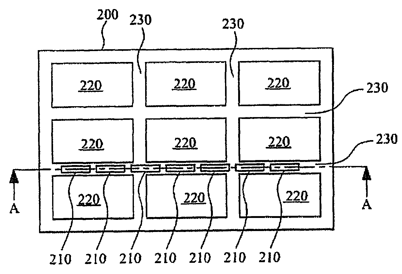
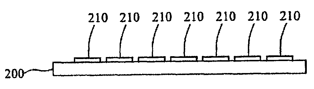
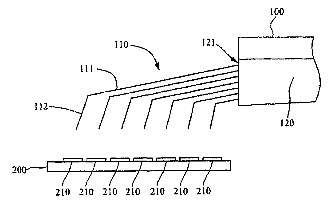
[0045] see figure 1 , 2 , 3 and 4, it is a wafer acceptance test method disclosed by the embodiment of the present invention, which is through the relative contact between the cantilever probe 110 of the probe card 100 and the contact pad 210 of the wafer 200. Position configuration, so that each cantilever probe 110 can definitely contact its corresponding contact pad 210 with an appropriate contact pressure, and the needle tip will not move out of the contact pad 110 due to the compression deformation of the cantilever probe 110 .

[0046] The wafer 200 used in the present invention forms a plurality of electronic components arranged in an array on the surface of the wafer 200 after the semiconductor component process. The multiple electronic components need to be further tested to determi...


PUM


Abstract

The invention discloses a wafer acceptance testing method, contact mats and a probe card. The wafer acceptance testing method comprises the following steps: firstly, providing a wafer and forming a plurality of devices to be tested and a plurality of scribe lines on the wafer, wherein the devices to be tested are parted by the scribe lines; secondly, arranging at a plurality of strip contact mats linearly in at least one scribe line, wherein the length of the contact mats is greater than the width of the scribe lines and the wide of the contact mats is smaller than the width of the scribe lines; and arranging a plurality of cantilever type probes, arranging the tips of the probes in the same line, and contacting the tips of the probes with the contact mats to test the electrical property of the wafer.

Description

technical field [0001] The present invention is related to Wafer Acceptable Test (WAT), in particular to a wafer acceptance test method which uses a cantilever probe to test a wafer and can effectively improve the utilization rate of the wafer surface area. Background technique [0002] Wafer Acceptable Test (WAT) refers to the test structure in which the semiconductor probes are used to feed test signals into the wafer after all processes are completed. By analyzing the feedback signals, the electrical characteristics of the wafer can be understood. In order to know whether there are defects in the wafer during fabrication. [0003] In order to feed the test signal into the probe, the test structure and the contact pads electrically connected to the test structure are formed in the process. The contact pad is used for contacting the tip of the probe, so that the probe is electrically connected with the test structure. Generally speaking, in order to cut the semi-finished ...

Claims


Application Information

Patent Timeline
Patent Type & Authority Applications(China)
IPC IPC(8): G01R31/28G01R31/26G01R1/073
Inventor 杨金田林顺泉杨惠彬
Owner MPI CORP
Why Eureka
Try Eureka