Method for removing residual photoresist

A technology of photoresist and photoresist layer, applied in photosensitive material processing, electrical components, semiconductor/solid-state device manufacturing, etc., can solve photoresist residue, affect the uniformity of the second ion implantation and the second doping area, etc. question

Active Publication Date: 2009-11-25
SEMICONDUCTOR MANUFACTURING INTERNATIONAL (BEIJING) CORP
View PDF1 Cites 12 Cited by
  • Summary
  • Abstract
  • Description
  • Claims
  • Application Information

AI Technical Summary

Problems solved by technology

[0005] In the above method, the pattern edge of the second photoresist layer produces photoresist residue, which in turn affects the uniformity of the second ion implantation into the second doped region

Method used


Image

  • Method for removing residual photoresist
  • Method for removing residual photoresist
  • Method for removing residual photoresist

Examples


Embodiment Construction

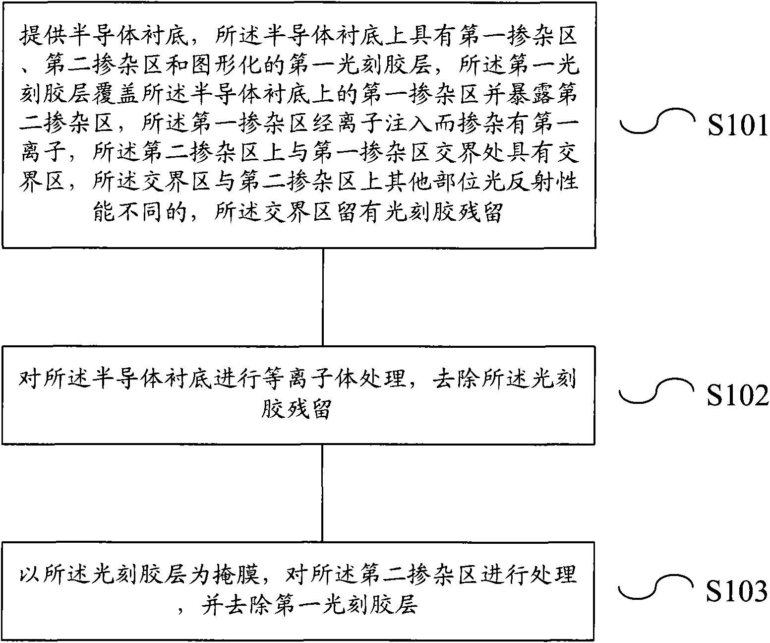
[0017] In this embodiment, plasma treatment is used to remove the photoresist residue left in the doped area to prevent the photoresist residue from affecting the subsequent processing of the second doped area.

[0018] To this end, this embodiment provides a method for removing photoresist residues, which includes the steps of: providing a semiconductor substrate having a first doped region, a second doped region, and a patterned photoresist on the semiconductor substrate. Layer, the photoresist layer covers the first doped region on the semiconductor substrate and exposes the second doped region, the first doped region is doped with first ions by ion implantation, the first There is a boundary area at the boundary between the second doped area and the first doped area. If the light reflection performance of the boundary area is different from other parts of the second doped area, the boundary area is left with photoresist residue; Plasma treatment is performed on the semiconduct...


PUM


Abstract

The invention provides a method for removing residual photoresist, which comprises the following steps: providing a semiconductor substrate; performing plasma treatment on the semiconductor substrate to remove the residual photoresist; and taking a photoresist layer as a mask to treat a second doped region and remove the photoresist layer, wherein the semiconductor substrate is provided with a first doped region, a second doped region and a graphic photoresist layer; the photoresist layer covers the first doped region on the semiconductor substrate and exposes the second doped region; the first doped region is doped with first ions by injecting ions; a junction region is arranged at the junction of the second doped region and the first doped region; the junction region has different light reflection performances with other parts of the second doped region; and the junction region is reserved with the residual photoresist. The residual photoresist generated by the difference of the light reflection performances on the junction region is removed by the method, and the influence of the residual photoresist on the process of the second doped region for subsequent treatment is prevented.

Description

Technical field [0001] The invention relates to a semiconductor manufacturing process, in particular to a method for removing photoresist residues. Background technique [0002] The doped regions defining the source and drain extension regions of the MOS device include a lightly doped drain (LDD) region and a pocket ion implantation region. The LDD impurity is located under the gate and close to the edge of the channel region, and the Pocket impurity is located under the LDD and close to the edge of the channel region, providing an impurity concentration gradient for the source and drain regions. [0003] The ion implantation method is generally used to dope the doped region. Ion implantation is a common technique for introducing dopant materials that change conductivity into a semiconductor substrate. In the ion implantation system, the required dopant material is ionized in the ion source, and the ions are accelerated into an ion beam with a prescribed energy and then directed ...

Claims


Application Information

Patent Timeline
Patent Type & Authority Applications(China)
IPC IPC(8): H01L21/02H01L21/027H01L21/266H01L21/336G03F7/42
Inventor 韩秋华马擎天
Owner SEMICONDUCTOR MANUFACTURING INTERNATIONAL (BEIJING) CORP
Why Eureka
Try Eureka