A semiconductor device and a semiconductor integrated circuit device
A semiconductor and circuit technology, applied in the field of semiconductor integrated circuit devices, can solve the problems of reducing, not getting enough EMI noise, and not being able to form an RC filter, etc., to achieve the effect of suppressing EMI noise and reducing EMI noise
- Summary
- Abstract
- Description
- Claims
- Application Information
AI Technical Summary
Problems solved by technology
Method used
Image
Examples
Embodiment 1
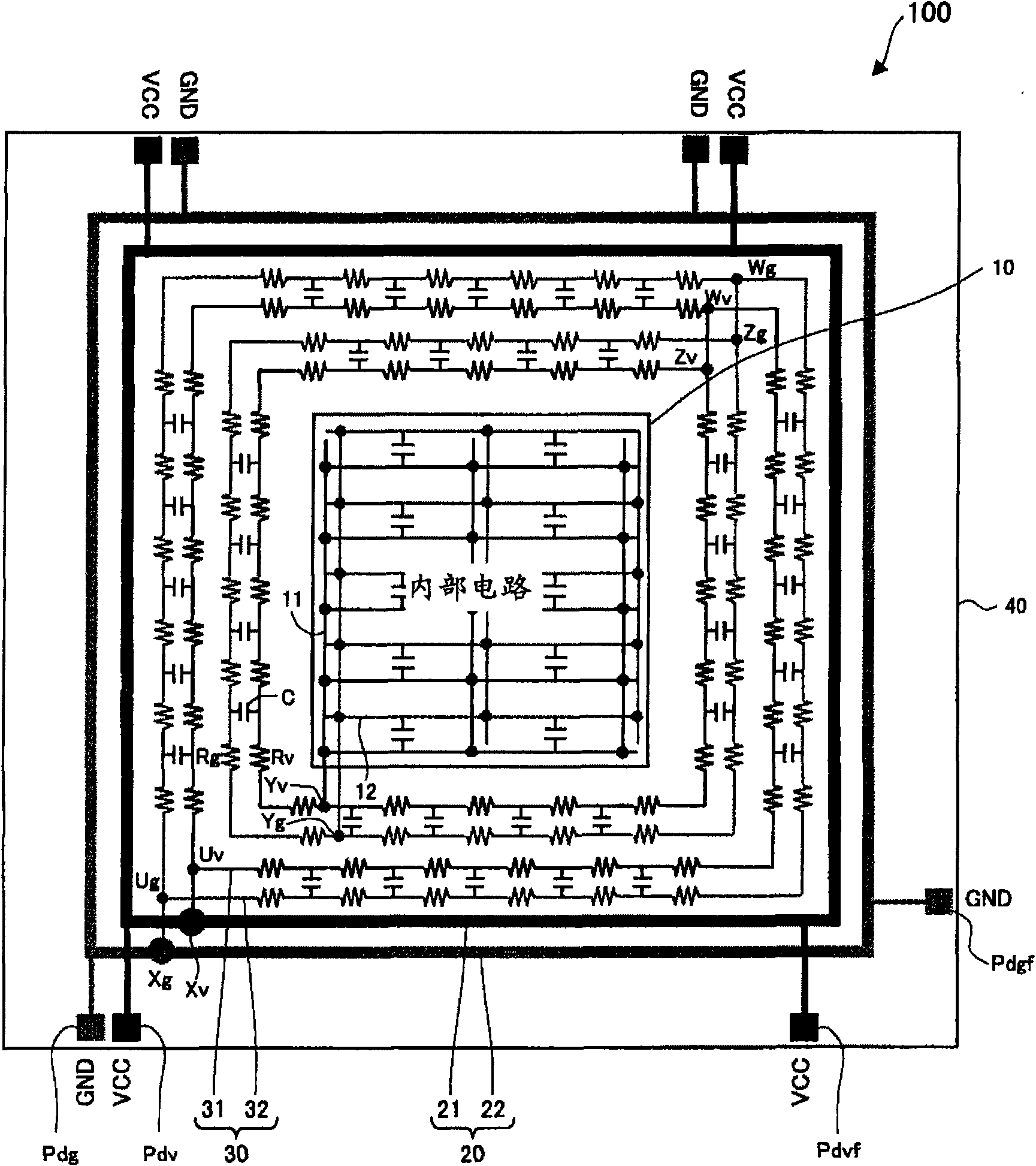
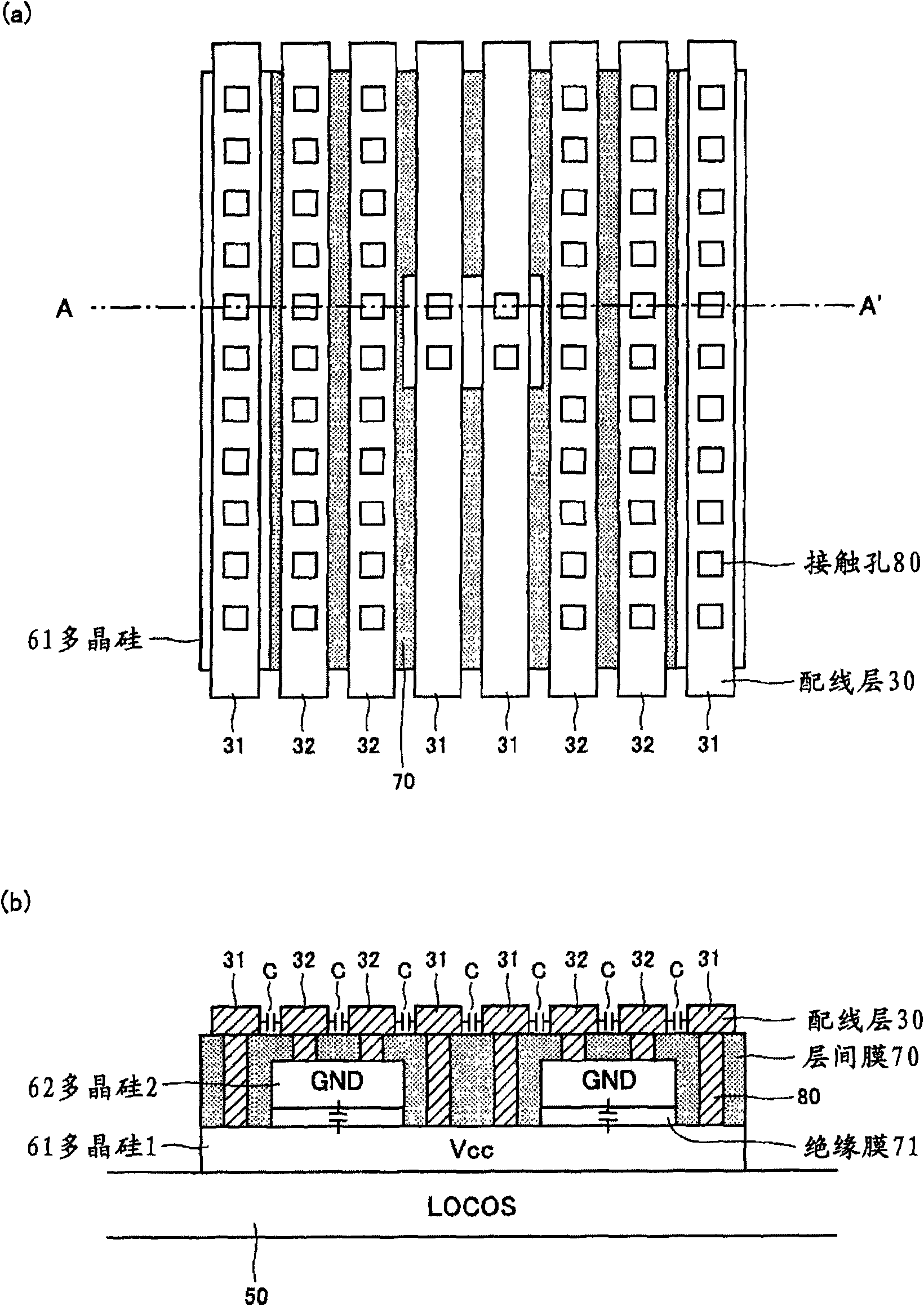
[0061] figure 1 It is an example of the overall configuration diagram of the semiconductor device 100 according to the first embodiment of the present invention. The semiconductor device 100 of the first embodiment has an internal circuit 10 , power terminal pads Pdv, ground terminal pads Pdg, peripheral power supply wiring 20 , and internal circuit supply power supply wiring 30 on a semiconductor wafer 40 . The peripheral power supply wiring 20 has a peripheral power supply wiring 21 for a power supply potential and a peripheral power supply wiring 22 for a ground potential. In addition, the internal circuit supply power supply wiring 30 has an internal circuit power supply potential supply wiring 31 and an internal circuit ground potential supply wiring 32 .
[0062] The internal circuit 10 is a circuit having predetermined processing functions of the semiconductor device 100 . The internal circuit 10 is provided on the semiconductor wafer 40 and performs predetermined fun...
Embodiment 2
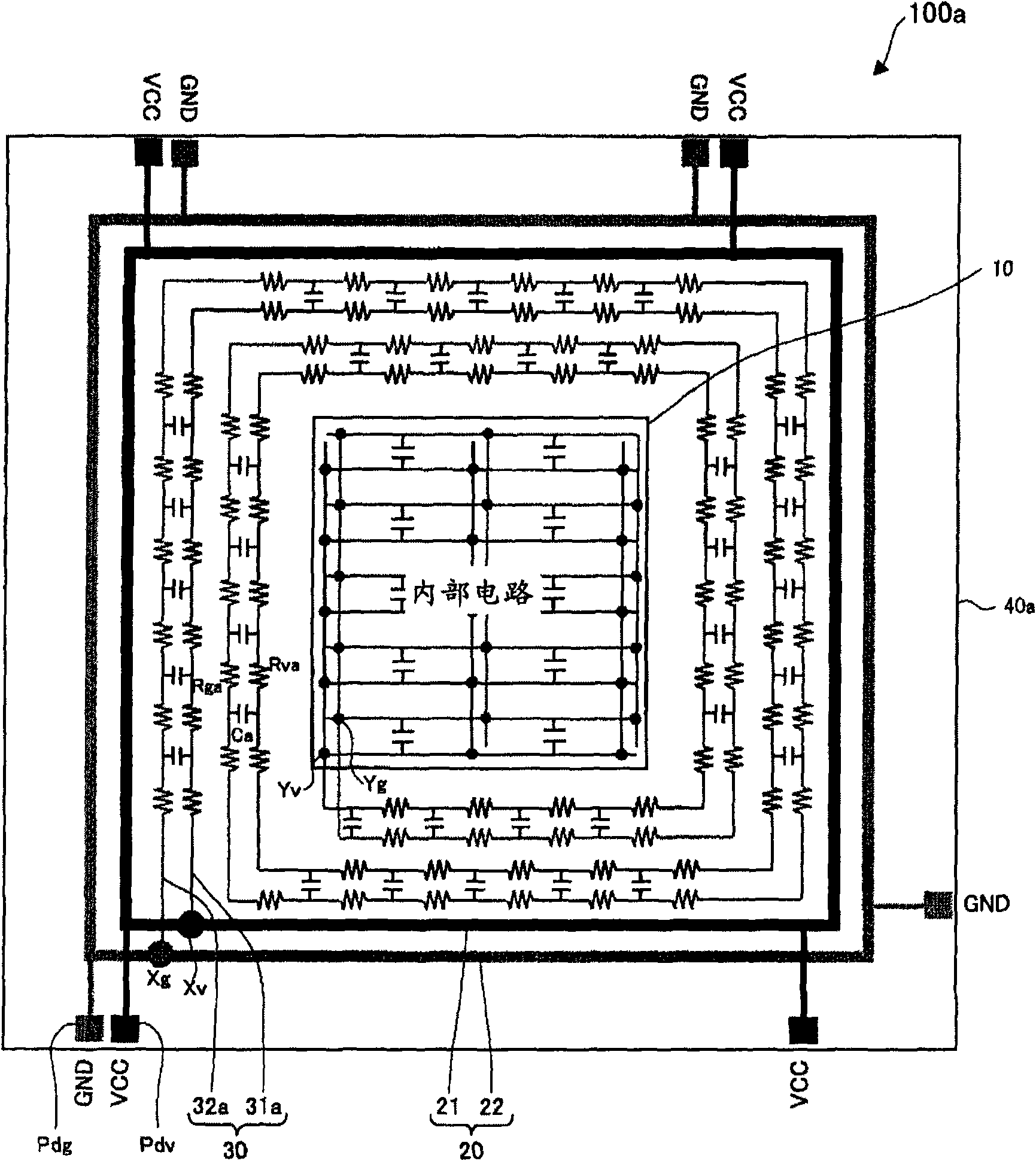
[0097] image 3 It is an example of an overall configuration diagram of a semiconductor device 100a according to Embodiment 2 of the present invention. In the semiconductor device 100a of the second embodiment, the arrangement structure of the power terminal pad Pdv, the ground terminal pad Pdg, the peripheral power supply wiring 20, and the internal circuit 10 is the same as that of the semiconductor device 100 of the first embodiment, so the same reference numerals are assigned and omitted. illustrate.
[0098] In the semiconductor device 100a of the second embodiment, the internal circuit supply power supply wiring 30a formed on the semiconductor wafer 40a has no parallel circuit part, and all of them are composed of RC distributed constant circuits, and the planar structure is spiral, which is different from that of the first embodiment. The semiconductor device 100 is different.
[0099] In Embodiment 2, among the power supply wiring 30a for internal circuit supply, the...
Embodiment 3
[0103] Figure 4 It is an example of an overall configuration diagram of a semiconductor device 100b according to Embodiment 3 of the present invention. exist Figure 4 In the semiconductor device 100b of the third embodiment, the arrangement and structure of the power terminal pad Pdv, the ground terminal pad Pdg, and the peripheral power supply wiring 20 are the same as those of the semiconductor devices 100 and 100a of the first and second embodiments. The description of the same reference symbols is omitted.
[0104] In the semiconductor device 100b of the third embodiment, the internal circuit 10b is not located in the center of the semiconductor wafer 40b, but is placed close to the side adjacent to the peripheral power supply wiring 20, which is different from the semiconductor devices of the first and second embodiments. 100, 100a are different. In this way, the semiconductor device 100b of this embodiment can be suitably applied even when the position where the int...
PUM
 Abstract
Description
Claims
Application Information


