A semiconductor device and a semiconductor integrated circuit device

A semiconductor and circuit technology, applied in the field of semiconductor integrated circuit devices, can solve the problems of reducing, not being able to obtain enough EMI noise, and not being able to form an RC filter, etc., to achieve the effect of reducing EMI noise and suppressing EMI noise

Active Publication Date: 2013-07-31
MITSUMI ELECTRIC CO LTD
View PDF1 Cites 0 Cited by
  • Summary
  • Abstract
  • Description
  • Claims
  • Application Information

AI Technical Summary

Problems solved by technology

[0004] However, in the structure described in the above-mentioned Patent Document 1, there is a problem that the circuit part is connected in the middle of the RC filter on a plane, so there is a part where the RC filter cannot function, and there is a problem that sufficient EMI noise cannot be obtained. Lowered Circuit Section
[0005] In addition, in the configuration described in Patent Document 1, a plurality of circuit parts are connected to the same RC filter, and therefore, it is not possible to independently form an RC filter that exhibits the maximum effect for each circuit part.

Method used


Image

  • A semiconductor device and a semiconductor integrated circuit device
  • A semiconductor device and a semiconductor integrated circuit device
  • A semiconductor device and a semiconductor integrated circuit device

Examples


Embodiment 1

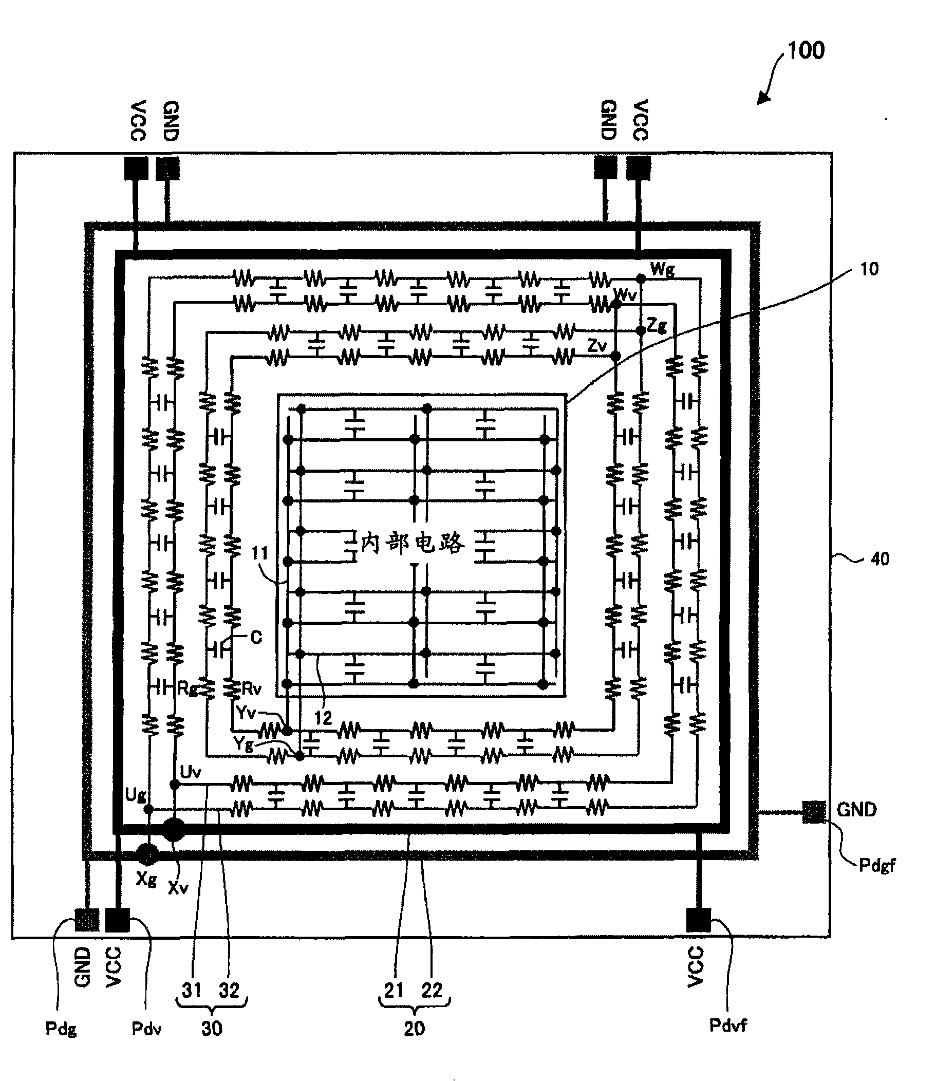
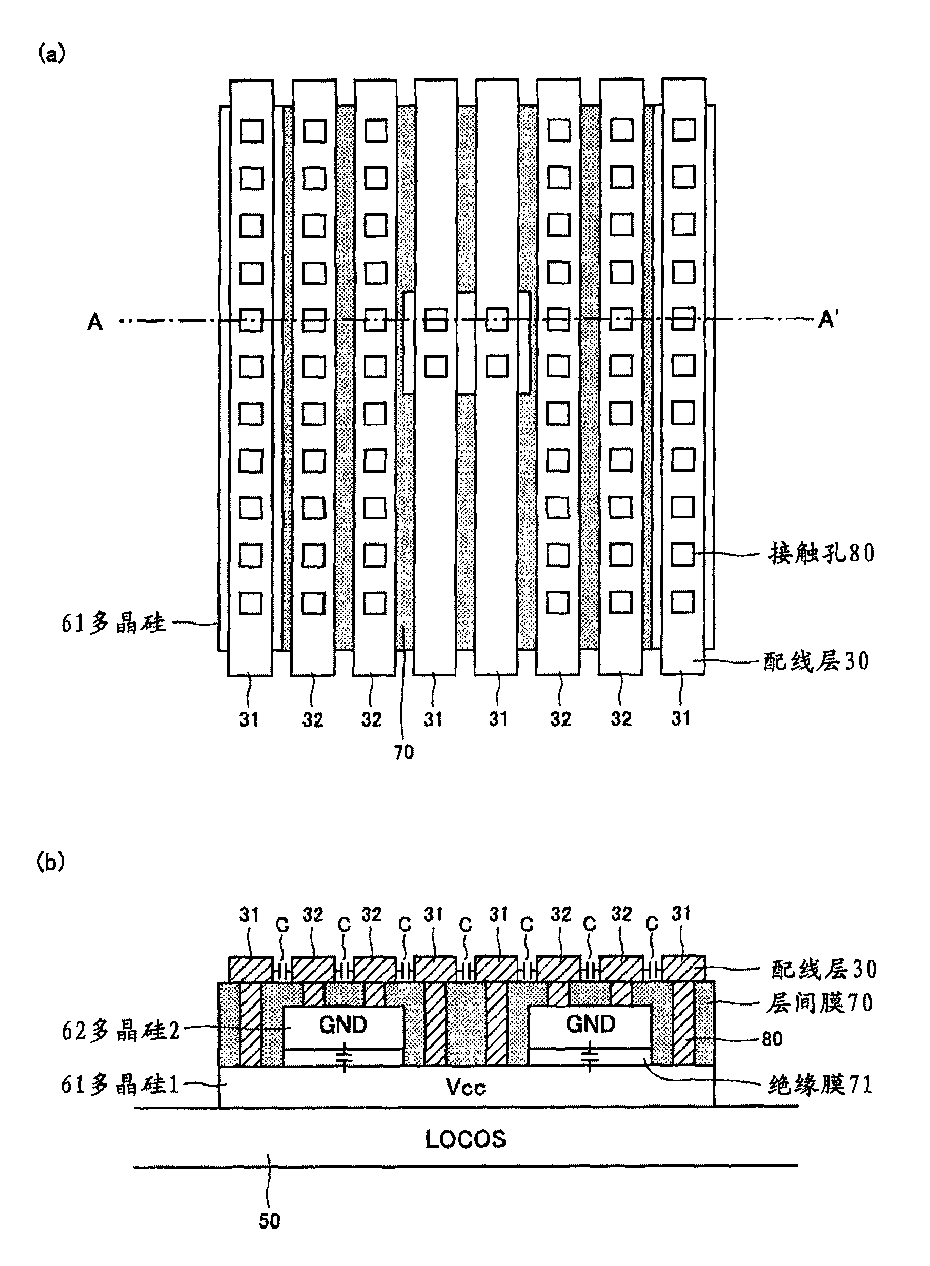
[0061] figure 1 It is an example of the overall configuration diagram of the semiconductor device 100 according to the first embodiment of the present invention. The semiconductor device 100 of the first embodiment has an internal circuit 10 , power terminal pads Pdv, ground terminal pads Pdg, peripheral power supply wiring 20 , and internal circuit supply power supply wiring 30 on a semiconductor wafer 40 . The peripheral power supply wiring 20 has a peripheral power supply wiring 21 for a power supply potential and a peripheral power supply wiring 22 for a ground potential. In addition, the internal circuit supply power supply wiring 30 has an internal circuit power supply potential supply wiring 31 and an internal circuit ground potential supply wiring 32 .

[0062] The internal circuit 10 is a circuit having predetermined processing functions of the semiconductor device 100 . The internal circuit 10 is provided on the semiconductor wafer 40 and performs predetermined fun...

Embodiment 2

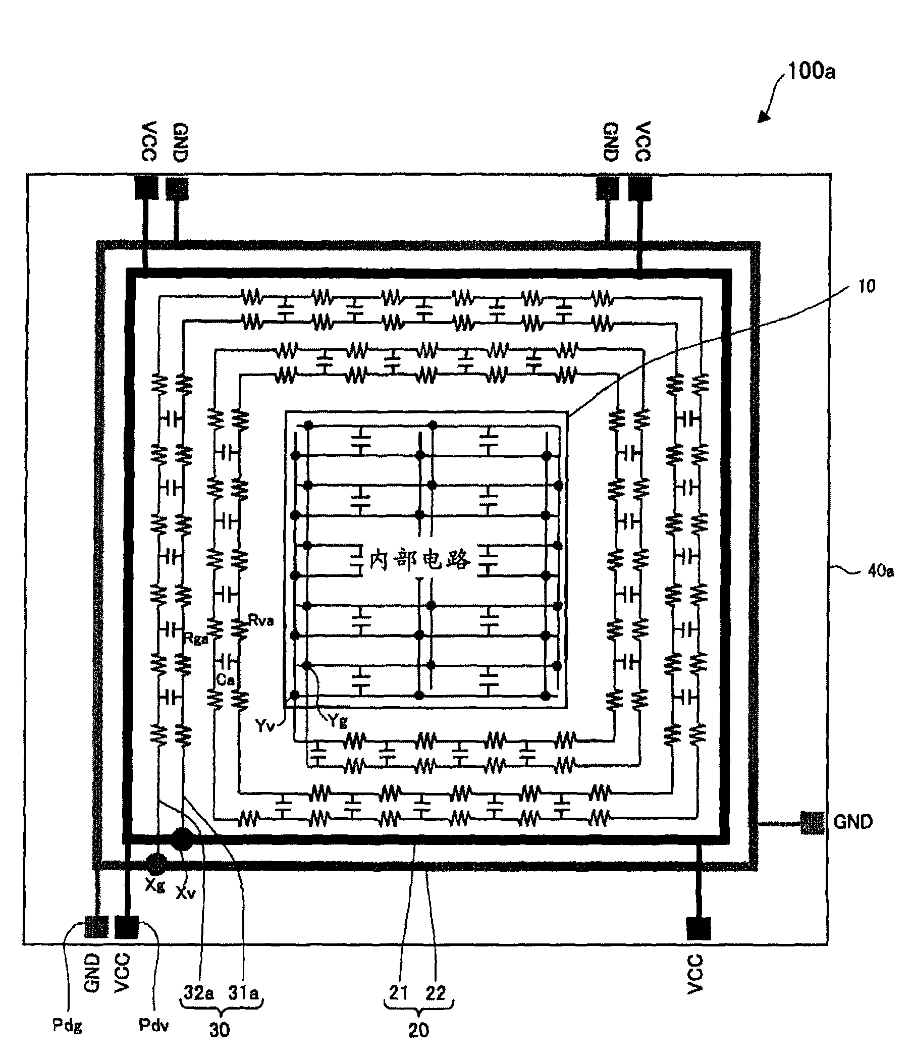
[0097] image 3 It is an example of an overall configuration diagram of a semiconductor device 100a according to Embodiment 2 of the present invention. In the semiconductor device 100a of the second embodiment, the arrangement structure of the power terminal pad Pdv, the ground terminal pad Pdg, the peripheral power supply wiring 20, and the internal circuit 10 is the same as that of the semiconductor device 100 of the first embodiment, so the same reference numerals are assigned and omitted. illustrate.

[0098] In the semiconductor device 100a of the second embodiment, the internal circuit supply power supply wiring 30a formed on the semiconductor wafer 40a has no parallel circuit part, and all of them are composed of RC distributed constant circuits, and the planar structure is spiral, which is different from that of the first embodiment. The semiconductor device 100 is different.

[0099] In Embodiment 2, among the power supply wiring 30a for internal circuit supply, the...

Embodiment 3

[0103] Figure 4 It is an example of an overall configuration diagram of a semiconductor device 100b according to Embodiment 3 of the present invention. exist Figure 4 In the semiconductor device 100b of the third embodiment, the arrangement and structure of the power terminal pad Pdv, the ground terminal pad Pdg, and the peripheral power supply wiring 20 are the same as those of the semiconductor devices 100 and 100a of the first and second embodiments. The description of the same reference symbols is omitted.

[0104] In the semiconductor device 100b of the third embodiment, the internal circuit 10b is not located in the center of the semiconductor wafer 40b, but is placed close to the side adjacent to the peripheral power supply wiring 20, which is different from the semiconductor devices of the first and second embodiments. 100, 100a are different. In this way, the semiconductor device 100b of this embodiment can be suitably applied even when the position where the int...


PUM


Abstract

The invention provides a semiconductor device and a semiconductor integrated circuit device provided with a wiring graph that can lower down EMI noise at maximum, which is provided with the following components: an internal circuit; a power supply terminal mat that connects with the outside and locates outer than the internal circuit, and a peripheral power supply wiring that connects with an earth terminal mat and is supplied with a power supply electric potential and an earthing electric potential; wiring for the internal circuit power supply electric potential supply that set between the internal circuit and the peripheral power supply wiring and supplies the power supply electric potential from the peripheral power supply wiring to the internal circuit, and wiring for internal circuitearthing electric potential supply that supplies the earthing electric potential, characterized in that the wiring for the internal circuit power supply electric potential supply and the wiring for internal circuit earthing electric potential supply are deployed closely so as to generate wiring capacitance, and holds as one part with a joint point of the internal circuit and the peripheral power supply wiring.

Description

technical field [0001] The present invention relates to a semiconductor device and a semiconductor integrated circuit device, and more particularly, to a semiconductor device and a semiconductor integrated circuit device having internal circuits and peripheral power supply lines. Background technique [0002] Conventionally, there is known a semiconductor device including an RC filter and a circuit section, wherein the RC filter is formed of an inter-wiring capacitance and a wiring resistance, and the inter-wiring capacitance is provided on a dielectric layer as the most Between the power wiring of the upper wiring and the ground wiring which is the uppermost wiring layer formed separately from the power wiring, the wiring resistance is composed of the power wiring and the ground wiring; the circuit part is used in The wiring on the lower layer of the uppermost wiring connects circuits and components, electrically connects the power supply wiring to the high-potential power ...

Claims


Application Information

Patent Timeline
Patent Type & Authority Patents(China)
IPC IPC(8): H01L23/485H01L23/528H01L23/28
CPCH01L23/5222H01L23/552H01L27/0611
Inventor 汤浅雄一
Owner MITSUMI ELECTRIC CO LTD
Why Eureka
Try Eureka