
Power device control circuit and power device circuit

a control circuit and power device technology, applied in pulse generators, pulse techniques, instruments, etc., can solve the problems of scale increase of control circuits, cost increase, and fear of adverse effects on peripheral devices and the like, and achieve the suppression of switching loss and emi noise suppression, low cost, and low cost

Active Publication Date: 2015-11-10
MITSUBISHI ELECTRIC CORP
View PDF20 Cites 0 Cited by
  • Summary
  • Abstract
  • Description
  • Claims
  • Application Information

AI Technical Summary

Benefits of technology

The present invention provides a power device control circuit that can make high-speed switching while achieving both suppression of switching loss and suppression of EMI noise. This control circuit drives the device with low power at the start and then increases the power as the device reaches its maximum speed. By changing the driving power in a relatively small scale circuit, monitoring of a gate voltage is not required, and the control circuit does not involve feedback control. This makes it possible to respond to high-speed switching.

Problems solved by technology

However, increasing a current and a voltage to be applied to the gate during switching increases EMI (electromagnetic interference) noise, resulting in the fear of adverse effect on a peripheral device and the like.
As described above, it is difficult to achieve both suppression of switching loss and suppression of EMI noise.
The aforementioned technique of Japanese Patent Application Laid-Open No. 2007-166655 requires a circuit to monitor the gate voltage and a circuit to protect the previous circuit from a surge voltage and the like, leading to the problems of scale increase of a control circuit and cost increase.
Control to monitor the gate voltage and feed the gate voltage back to the control circuit involves a certain period of time for the feedback, making it impossible to respond to high-speed switching.

Method used


Image

  • Power device control circuit and power device circuit
  • Power device control circuit and power device circuit
  • Power device control circuit and power device circuit

Examples


first preferred embodiment

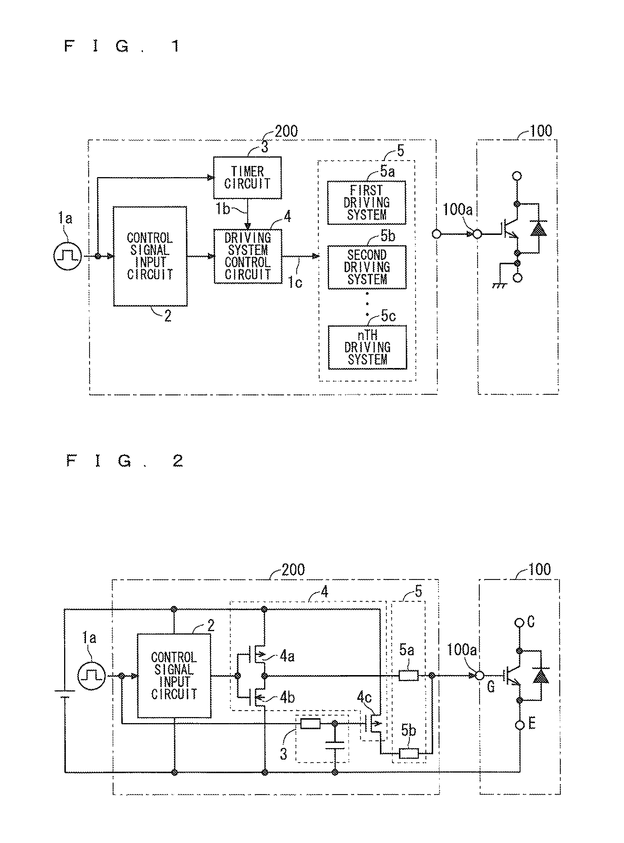
[0026]FIG. 1 is a block diagram of a power device control circuit of a first preferred embodiment. A gate terminal 100a of a power device 100 targeted for control is connected to a power device control circuit 200. The power device 100 is an IGBT to which a free-wheel diode is connected, for example.

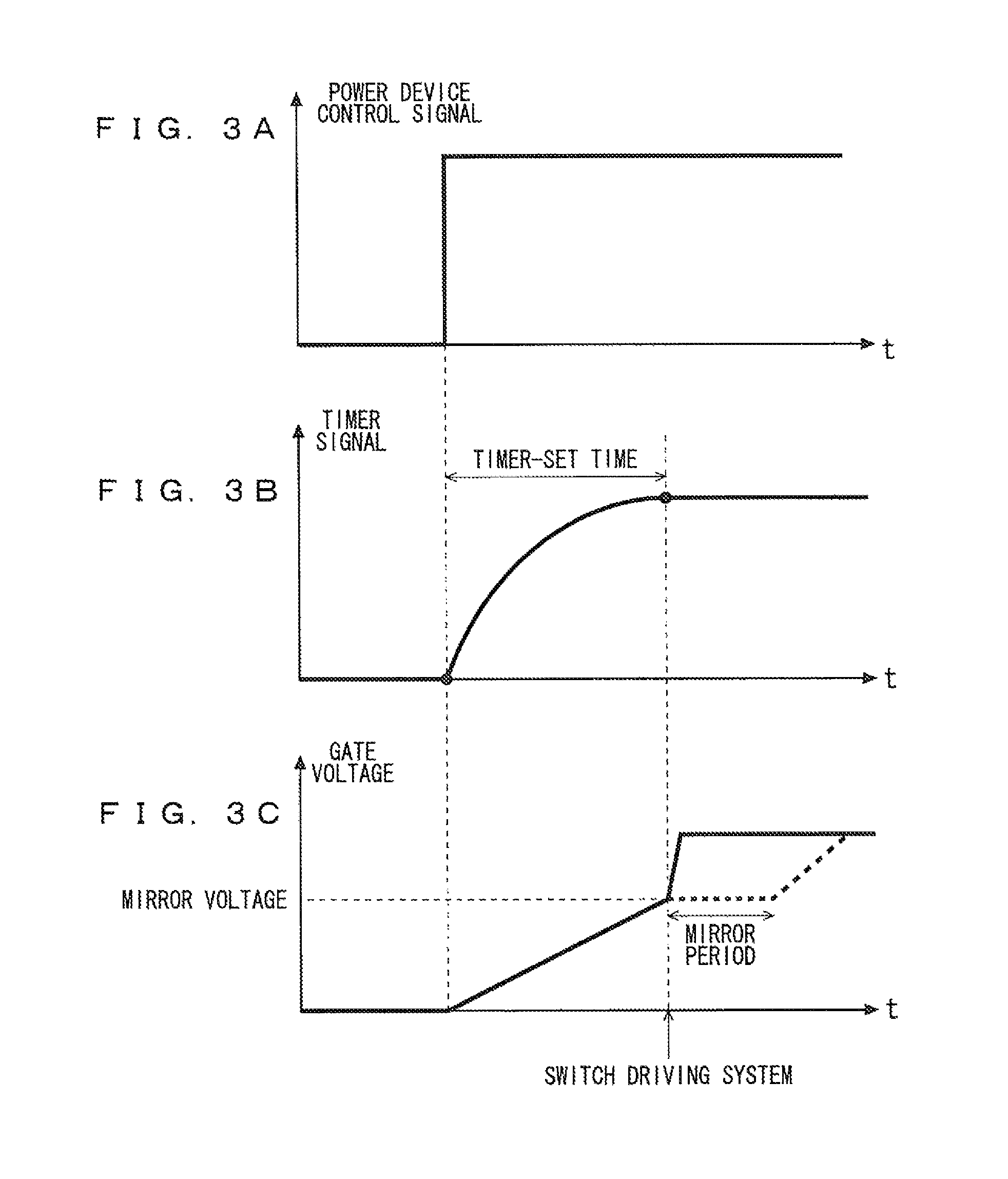
[0027]A control signal input circuit 2 that receives a power device control signal 1a applied from outside is connected to a driving system control circuit 4. A timer circuit 3 makes a count for time elapsed until a gate voltage reaches a mirror voltage in response to the power device control signal 1a, and enters a timer signal 1b into the driving system control circuit 4.

[0028]A driving circuit 5 is connected to the driving system control circuit 4, and receives a driving circuit control signal 1c from the driving system control circuit 4. The output of the driving circuit 5 is entered into the gate terminal 100a of the power device 100.

[0029]The driving circuit 5 has a plurality of dr...

second preferred embodiment

[0046]FIG. 4 is a block diagram of a power device control circuit 200 of a second preferred embodiment. In the first preferred embodiment, a signal to be entered into the timer circuit 3 is the power device control signal 1a. Unlike in the first preferred embodiment, the driving circuit control signal 1c is entered into the timer circuit 3. The circuit structure of the second preferred embodiment is the same as that of the first preferred embodiment in other respects, so the same structure will not be described repeatedly.

[0047]Like that of the first preferred embodiment, the timer circuit 3 of FIG. 4 is a time constant circuit. The timer circuit 3 is set in advance such that time during which the timer circuit 3 makes a count agrees with time elapsed until a gate voltage reaches a mirror voltage.

[0048]FIGS. 5A to 5C show the sequence of operation of the power device control circuit 200 of the second preferred embodiment. In the first preferred embodiment (FIGS. 3A to 3C), the timer...

third preferred embodiment

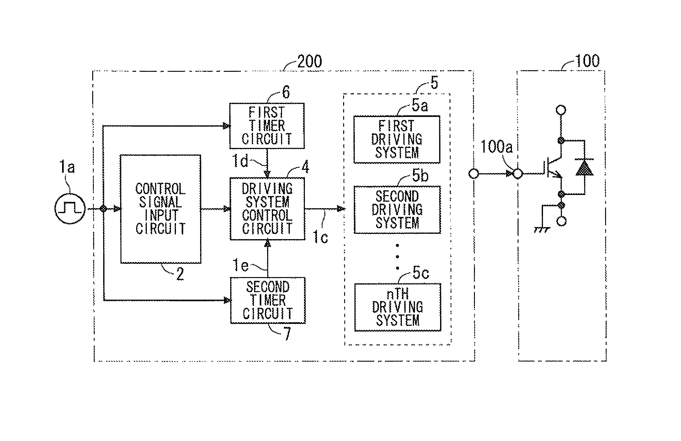
[0050]FIG. 6 is a block diagram of a power device control circuit 200 of a third preferred embodiment. Unlike in the first and second preferred embodiments, two timer circuits including first and second timer circuits 6 and 7 are provided. Time during which the first timer circuit 6 makes a count and time during which the second timer circuit 7 makes a count are shifted to generate a time difference between time when a timer signal 1d is entered into the driving system control circuit 4 and time when a timer signal 1e is entered into the driving system control circuit 4. By using this time difference, the first, second and nth driving systems 5a, 5b and 5c can be switched in a stepwise manner.

[0051]A plurality of timer circuits is provided in the power device control circuit 200 of the third preferred embodiment. Thus, switching between the driving systems can be performed several times to allow change of driving power more smoothly than the first and second preferred embodiments, t...


PUM


Abstract

A power device control circuit enters a gate driving signal into a gate terminal of a power device. The power device control circuit includes: a control signal input circuit that receives a power device control signal for control of the power device; a driving system control circuit connected to the control signal input circuit; a driving circuit with a plurality of driving systems, the driving circuit driving the power device in response to a driving circuit control signal received from the driving system control circuit; and a timer circuit that makes switching between the driving systems in response to the driving circuit control signal after elapse of a given period of time from receipt of a predetermined signal, specifically the power device control signal, thereby changing the driving power of the driving system control circuit to drive the power device.

Description

BACKGROUND OF THE INVENTION[0001]1. Field of the Invention[0002]The present invention relates to a power device control circuit and more specifically, relates to a power device control circuit that enters a gate driving signal into a gate terminal of a power device.[0003]2. Description of the Background Art[0004]For drive of a power device such as an IGBT, a power device control circuit controls a gate signal of the power device to perform switching of the power device.[0005]During turn-on of the power device, transition from OFF condition to ON condition of the power device involves turn-on time. This turn-on time is time required for electrical charges to be accumulated in a gate-to-emitter capacitance and a gate-to-collector capacitance. In response to charging of these capacitances, a gate voltage is increased to reach a threshold voltage, thereby placing the power device in ON condition.[0006]There is a period when a gate-to-emitter voltage is constant during increase of the ga...

Claims


Application Information

Patent Timeline
Patent Type & Authority Patents(United States)
IPC IPC(8): H03B1/00H03K3/00G05F1/66H03K3/012
CPCG05F1/66H03K3/012H02M1/08H02M1/44H03K17/0406H03K17/162H03K17/168H03K2217/0036H02M1/0054Y02B70/10
Inventor UOTA, SHIORIINOUE, TAKAHIROTAMAKI, KOJIORITA, SHOICHI
Owner MITSUBISHI ELECTRIC CORP
Learn More