
Semiconductor device

a technology of semiconductor switching elements and capacitors, applied in the direction electrical equipment, basic electric elements, etc., can solve the problems of mainly caused power loss of semiconductor switching elements, method of reducing cgc while suppressing adverse effects on other characteristics, and method of reducing cgc has not been sufficiently studied so far, so as to achieve the effect of suppressing switching loss

Active Publication Date: 2021-04-06
MITSUBISHI ELECTRIC CORP
View PDF7 Cites 0 Cited by
  • Summary
  • Abstract
  • Description
  • Claims
  • Application Information

AI Technical Summary

Benefits of technology

The invention relates to a semiconductor device which has a layer for storing carriers while reducing switching loss. By using an internal insulating film with different thicknesses at different parts of the device, parasitic capacitance is reduced which leads to a reduction of switching loss. The technical effect of this invention is to provide a semiconductor device with improved performance.

Problems solved by technology

The power loss of semiconductor switching elements is mainly caused by ON-loss and switching loss.
However, for an IGBT having a carrier storage layer, a method of reducing Cgc while suppressing adverse effects on other characteristics has not been sufficiently studied so far.
More generally speaking, in a semiconductor device having a carrier storage layer, a method of reducing the parasitic capacitance while suppressing adverse effects on other characteristics has not been sufficiently studied so far.

Method used


Image

  • Semiconductor device
  • Semiconductor device
  • Semiconductor device

Examples


first preferred embodiment

[0036](Configuration)

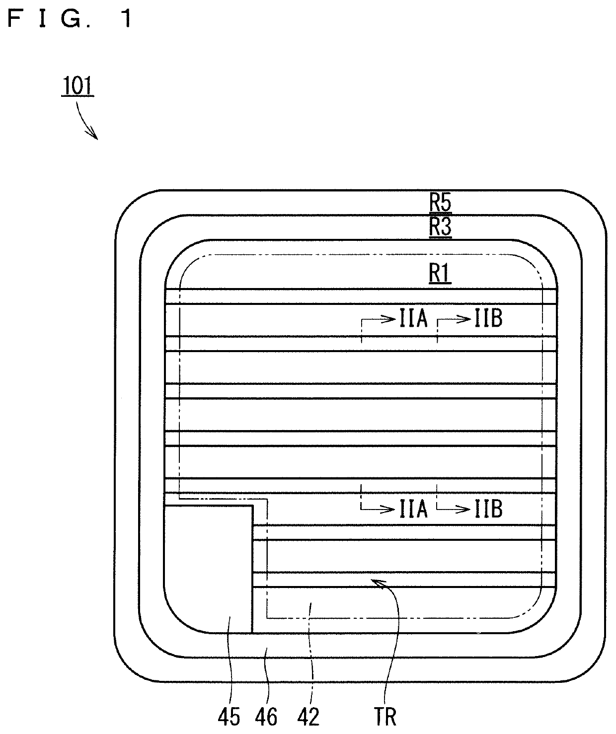
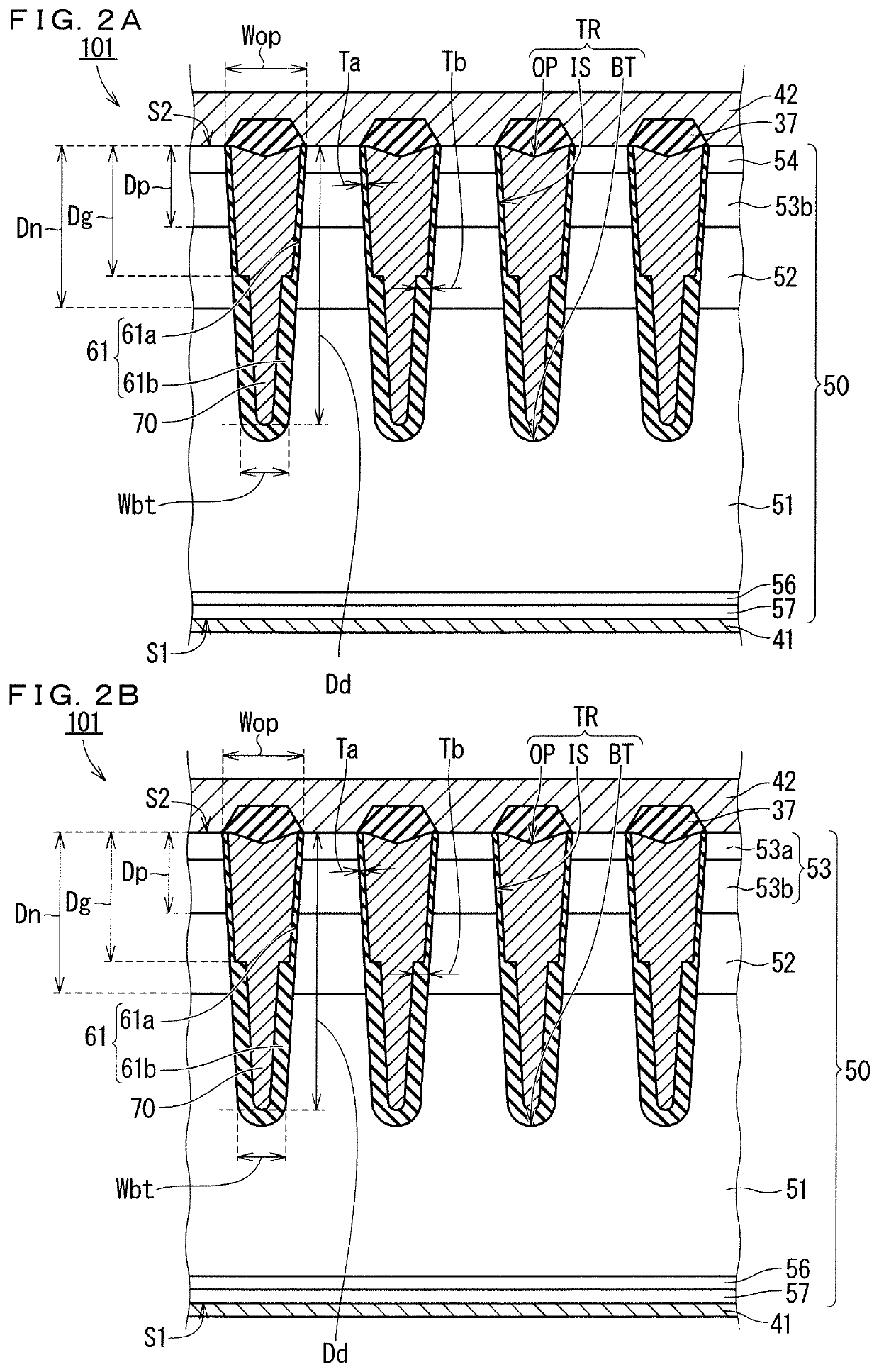
[0037]FIG. 1 is a top view schematically showing a configuration of an IGBT 101 (semiconductor device) in a first preferred embodiment. FIGS. 2A and 2B are partial cross-sectional views adjacent to each other in a cell region R1 (FIG. 1) of the IGBT 101, and specifically are partial cross-sectional views along line IIA-IIA and line IIB-IIB in FIG. 1. Meanwhile, in FIG. 1, an outer edge of an emitter electrode 42 (second main electrode) is exclusively shown by a two-dot chain line in order to make the drawing easily viewable.

[0038]The IGBT 101 has a semiconductor substrate 50, an internal insulating film 61, a trench electrode 70, a collector electrode 41 (first main electrode), the emitter electrode 42, and an interlayer insulating film 37. The semiconductor substrate 50 has a surface S1 (first surface) and a surface S2 (second surface) that is a surface opposite to the surface S1. In this specification, a “depth” in the semiconductor substrate 50 is defined as ...

second preferred embodiment

[0054](Configuration)

[0055]FIG. 11 is a partial cross-sectional view schematically showing a configuration of an IGBT 102 (semiconductor device) in a second preferred embodiment. Also in the IGBT 102, as in the IGBT 101 (FIGS. 2A and 2B: the first preferred embodiment), an internal insulating film 61 has a thickness Ta at a portion facing a p base layer 53, has a thickness Tb at a portion facing an n− drift layer 51, and has the thickness Ta and the thickness Tb at a portion facing an n carrier storage layer 52, and the thickness Tb is thicker than the thickness Ta. Further, in the present preferred embodiment, a portion of the internal insulating film 61 deeper than the deepest part of a trench electrode 70 has a thickness Tc (third thickness) thicker than the thickness Tb. Specifically, a lower portion 61b of the internal insulating film 61 has the thickness Tc thicker than the thickness Tb on a bottom part BT of a trench TR.

[0056]Note that, in this specification, the “thickness” ...

third preferred embodiment

[0060](Configuration)

[0061]FIG. 12 is a partial cross-sectional view schematically showing a configuration of an IGBT 201 (semiconductor device) in a third preferred embodiment. The IGBT 201 has a trench electrode 71 instead of the trench electrode 70 (FIG. 1: the first preferred embodiment). The trench electrode 71 has an upper electrode 71a and a buried electrode 71b. The upper electrode 71a is in contact with a portion of an internal insulating film 61 having a thickness Ta. The buried electrode 71b is in contact with a portion of the internal insulating film 61 having a thickness Tb. Specifically, the trench electrode 71 has the upper electrode 71a disposed shallower than a depth Dg, and the buried electrode 71b disposed deeper than the upper electrode 71a. The IGBT 201 has an isolation insulating film 63 that separates the upper electrode 71a and the buried electrode 71b in a trench TR. In the present preferred embodiment, the buried electrode 71b is electrically connected to t...


PUM

PropertyMeasurementUnit
conductivityaaaaaaaaaa
concentrationaaaaaaaaaa
conductivity typeaaaaaaaaaa

Abstract

A semiconductor substrate has a first surface and a second surface provided with an opening of a trench. A first-conductivity-type carrier storage layer is provided on the second surface side of a first-conductivity-type drift layer. A second-conductivity-type base layer is provided on the second surface side of the carrier storage layer and reaches the second surface. A first-conductivity-type impurity layer is provided on the second surface side of the base layer. A trench electrode is provided in the trench via an internal insulating film. The internal insulating film has a first thickness at a portion facing the base layer, has a second thickness at a portion facing the drift layer, and has the first thickness and the second thickness at a portion facing the carrier storage layer. The second thickness is thicker than the first thickness.

Description

BACKGROUND OF THE INVENTIONField of the Invention[0001]The present invention relates to a semiconductor device, and particularly to a semiconductor device having a trench electrode.Description of the Background Art[0002]Semiconductor switching elements (semiconductor devices) such as insulated gate bipolar transistors (IGBTs) are, for example, widely used for power modules for performing variable speed control of a three-phase motor, in the fields of general-purpose inverters and alternating current (AC) servos. From the viewpoint of energy saving, it is desired to reduce power loss of semiconductor switching elements. The power loss of semiconductor switching elements is mainly caused by ON-loss and switching loss.[0003]For example, according to Japanese Patent Application Laid-Open No. 2016-111077, an IGBT having a trench gate structure is disclosed. By applying the trench gate structure, ON-loss can be reduced by improving a channel density. Further, in the IGBT disclosed in Japa...

Claims


Application Information

Patent Timeline
Patent Type & Authority Patents(United States)
IPC IPC(8): H01L29/739H01L29/40H01L29/423
CPCH01L29/7397H01L29/407H01L29/4236H01L29/42376H01L29/4238
Inventor NISHI, KOICHI
Owner MITSUBISHI ELECTRIC CORP
Learn More