Semiconductor device and method of forming a semiconductor device
A semiconductor and device technology, applied in the field of semiconductor devices, can solve problems such as increasing the cost of manufacturing devices
- Summary
- Abstract
- Description
- Claims
- Application Information
AI Technical Summary
Problems solved by technology
Method used
Image

Examples
Embodiment Construction
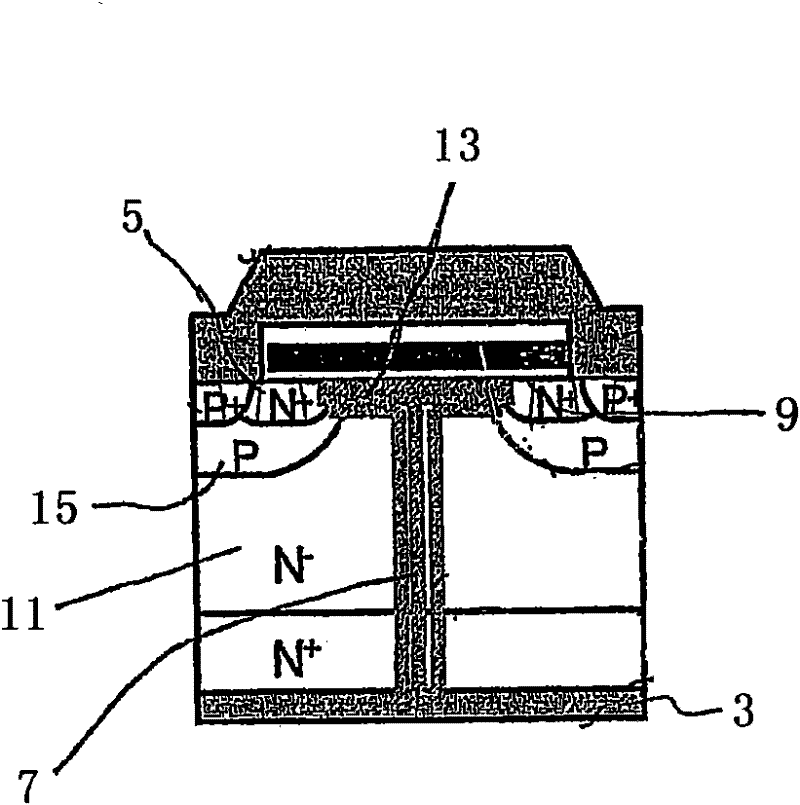
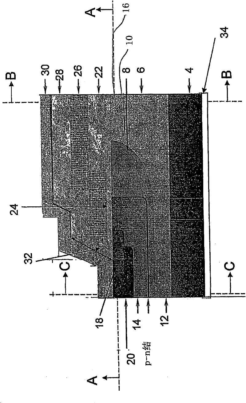
[0021] described below and in Figure 2 to Figure 9 , designate certain areas as specific materials, conductivity, and / or types. However, this is for ease of explanation only and is not intended to be limiting. From the description given herein, those skilled in the art will understand that to obtain different device functions, different semiconductor materials can be used, and the doping of different regions of the device can be changed.
[0022] The present disclosure will be described with reference to semiconductor devices including vertical semiconductor devices such as N-channel vertical MOSFET devices. A vertical semiconductor device includes a source electrode positioned above a drain electrode such that current flows primarily in a vertical direction when the device is in an on state. It should be understood that the present disclosure is not limited to vertical devices nor to N-channel MOSFET devices, and applies equally to other semiconductor devices such as later...
PUM
 Abstract
Description
Claims
Application Information
 - R&D
- Intellectual Property
- Life Sciences
- Materials
- Tech Scout
- Unparalleled Data Quality
- Higher Quality Content
- 60% Fewer Hallucinations
Browse by: Latest US Patents, China's latest patents, Technical Efficacy Thesaurus, Application Domain, Technology Topic, Popular Technical Reports.
© 2025 PatSnap. All rights reserved.Legal|Privacy policy|Modern Slavery Act Transparency Statement|Sitemap|About US| Contact US: help@patsnap.com