Active matrix display compensating method

A voltage source and source electrode technology, applied in the field of active matrix display devices, can solve the problems of reducing the aperture ratio and unusable bottom light-emitting devices, and achieve the effect of increasing complexity

Active Publication Date: 2009-12-02
GLOBAL OLED TECH
View PDF0 Cites 11 Cited by
  • Summary
  • Abstract
  • Description
  • Claims
  • Application Information

AI Technical Summary

Problems solved by technology

For bottom emitting devices where the aperture ratio is important, this additional circuitry reduces the aperture ratio and can even render such bottom emitting devices unusable

Method used


Image

  • Active matrix display compensating method
  • Active matrix display compensating method
  • Active matrix display compensating method

Examples


Embodiment Construction

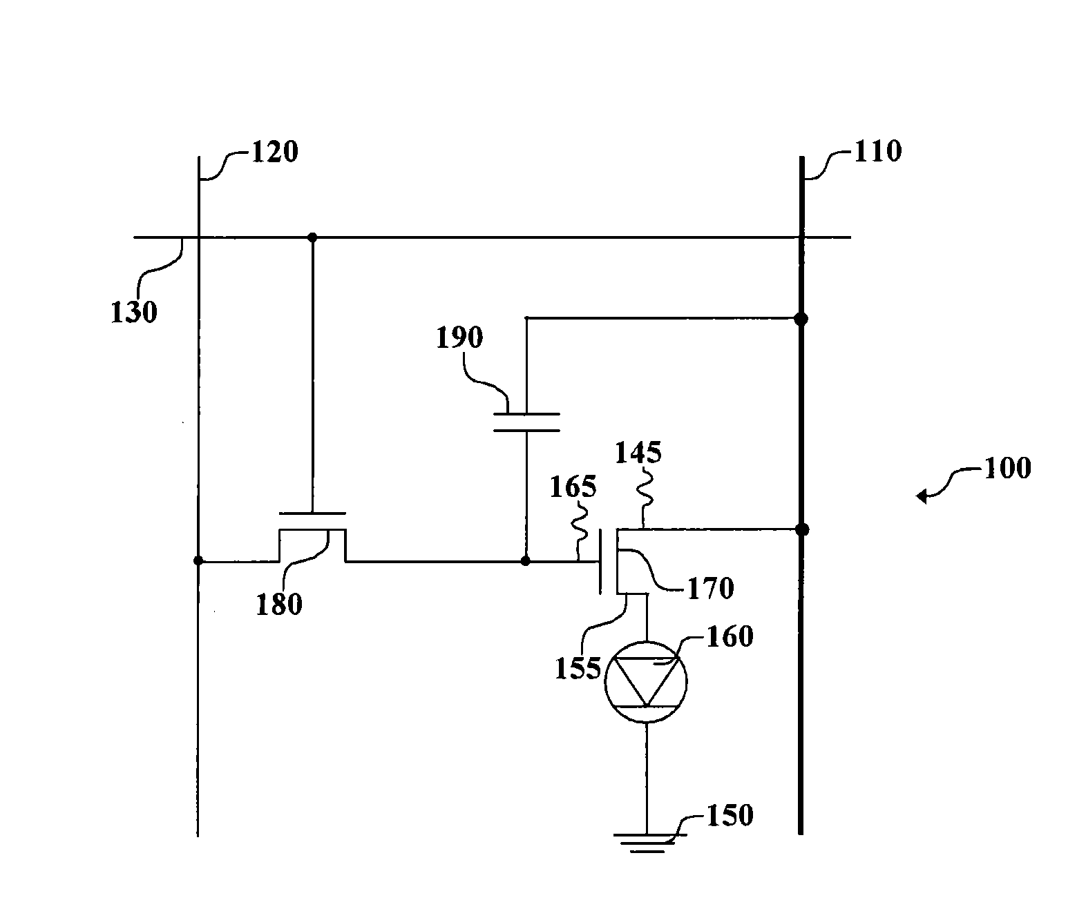
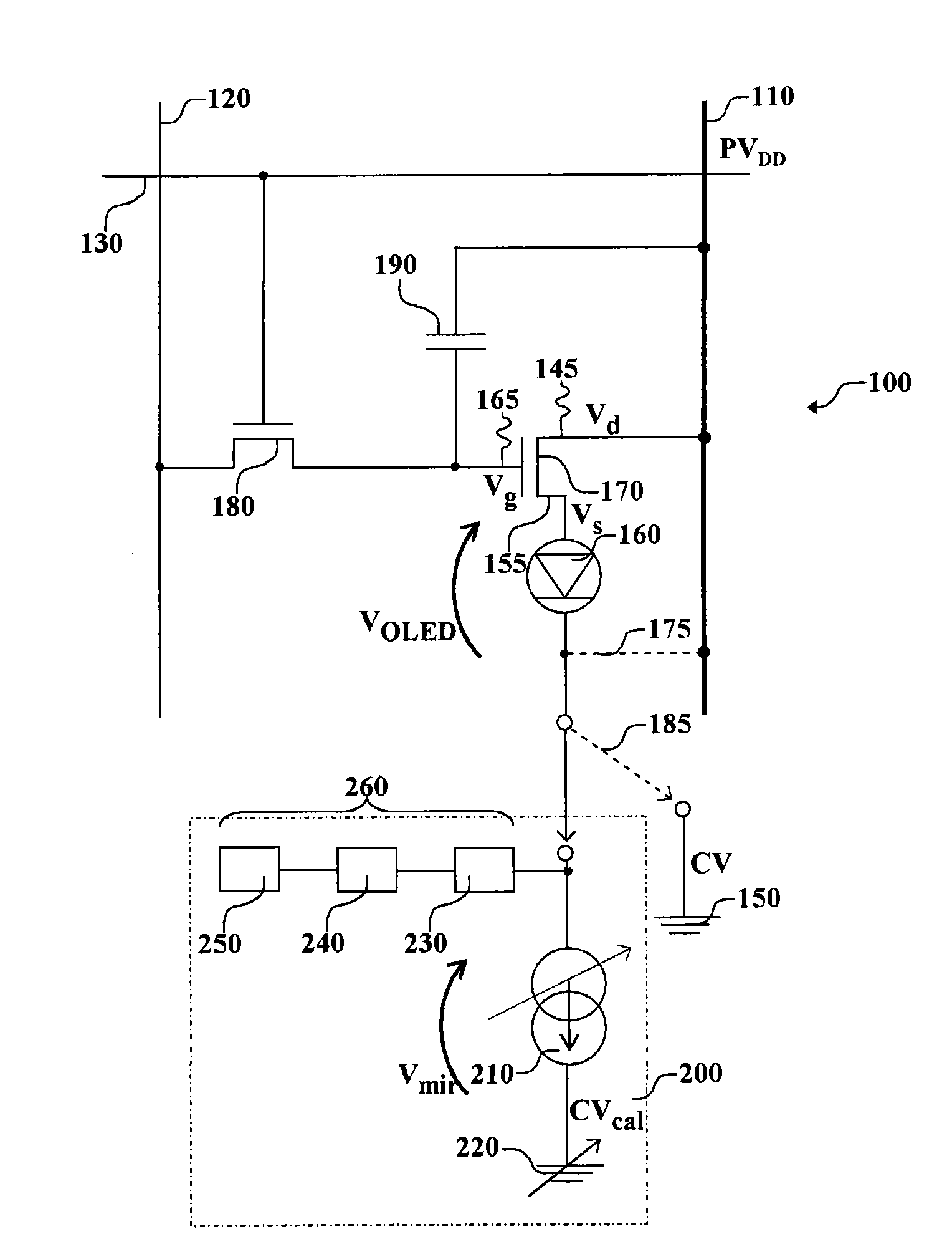
[0020] now go to figure 1 , shows a schematic diagram of one embodiment of an OLED driving circuit that can be used in the practice of the present invention. Such OLED driver circuits are well known in the technical field of active matrix OLED displays. OLED pixel drive circuit 100 has data line 120, supply line or first voltage source 110, select line 130, drive transistor 170, switching transistor 180, OLED device 160, which may be a single pixel of an OLED display, and capacitor 190. The driving transistor 170 is an amorphous silicon (a-Si) transistor and has a first electrode 145 , a second electrode 155 and a gate electrode 165 . The first electrode 145 of the drive transistor 170 is electrically connected to the first voltage source 110 , and the second electrode 155 is electrically connected to the OLED device 160 . In this embodiment of the pixel driving circuit 100, the first electrode 145 of the driving transistor 170 is a drain electrode, and the second electrode ...


PUM


Abstract

Compensating for changes in the threshold voltage of the drive transistor of an OLED drive circuit, the drive transistor includes a first electrode, second electrode, and gate electrode; connecting a first voltage source to the first electrode, and an OLED device to the second electrode and to a second voltage source; providing a test voltage to the gate electrode and connecting to the OLED drive circuit a test circuit that includes an adjustable current mirror causing voltage applied to the current mirror to be at a first test level; providing a test voltage to the gate electrode of the drive transistor and connecting the test circuit to the OLED device producing a second test level after the drive transistor and the OLED device age; and using the first and second test levels to calculate changes in the voltage applied to the gate electrode to compensate for drive transistor aging.

Description

technical field [0001] The present invention relates to an active matrix-type display device for driving display elements. Background technique [0002] In recent years, it has become necessary for image display devices to have high resolution and high image quality, and such image display devices are expected to have low power consumption, thinness, and wide-angle viewability. With such demands, display devices (displays) have been developed in which thin film active elements (thin film transistors, also referred to as TFTs) are formed on a glass substrate, and then display elements are formed thereon. [0003] In general, a substrate on which active elements are formed is such that interconnections and patterns formed using metal are provided after forming a semiconductor film of silicon, such as amorphous silicon or polycrystalline silicon. Since the electrical characteristics of the active elements are different, the former requires an integrated circuit (IC) for drivin...

Claims


Application Information

Patent Timeline
Patent Type & Authority Applications(China)
IPC IPC(8): G09G3/32
CPCG09G2320/0295G09G3/3233G09G2320/043
Inventor C·I·莱维J·W·哈默
Owner GLOBAL OLED TECH
Why Eureka
Try Eureka