Thin film transistor, method of manufacturing the same, and flat panel display device having the same

A thin-film transistor and flat-panel display technology, used in transistors, semiconductor/solid-state device manufacturing, electrical solid-state devices, etc., can solve problems such as poor ohmic contact and energy band gap width, and achieve improved electrical characteristics, reduced contact resistance, improved Effects of Current-Voltage Characteristics

Inactive Publication Date: 2009-12-23
SAMSUNG DISPLAY CO LTD
View PDF1 Cites 28 Cited by
  • Summary
  • Abstract
  • Description
  • Claims
  • Application Information

AI Technical Summary

Problems solved by technology

[0008] However, conventional thin film transistors using semiconductor oxides as active layers have poor ohmic contact with metal electrodes due to the wide bandgap of semiconductor oxides

Method used


Image

  • Thin film transistor, method of manufacturing the same, and flat panel display device having the same
  • Thin film transistor, method of manufacturing the same, and flat panel display device having the same
  • Thin film transistor, method of manufacturing the same, and flat panel display device having the same

Examples


Embodiment Construction

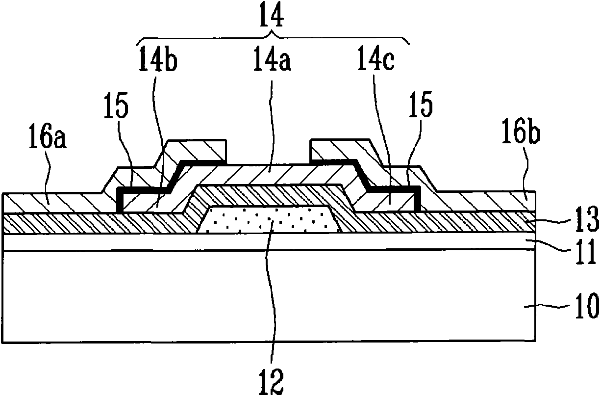
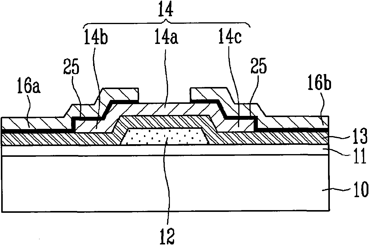
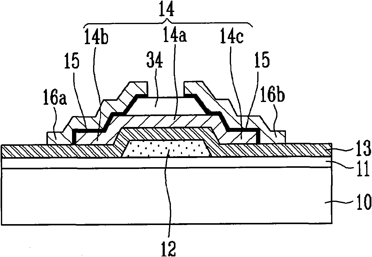
[0029] In the following detailed description, only certain exemplary embodiments of the present invention are shown and described, by way of illustration only. As those skilled in the art would realize, the described embodiments may be modified in various different ways, all without departing from the spirit or scope of the present invention. Accordingly, the drawings and description are to be regarded as illustrative in nature and not restrictive. In addition, when an element is referred to as being "on another element", "formed on another element" or "arranged on another element", it may be directly on another element, directly formed on another element , or directly on another element, or one or more intermediate elements may be arranged between them. Also, when an element is referred to as being "connected to," "connected to" or "electrically connected to" another element, it can be directly connected to the other element or indirectly connected to the other element and ...


PUM


Abstract

A thin film transistor, a method of manufacturing the same, and a flat panel display device having the thin film transistor, wherein the thin film transistor includes: an oxide semiconductor layer formed on a substrate and having a channel region, a source region, and a drain region; a gate electrode insulated from the oxide semiconductor layer by a gate insulating layer; an ohmic contact layer formed on the source region and the drain region of the oxide semiconductor layer; and a source electrode and a drain electrode coupled to the source region and the drain region through the ohmic contact layer, the ohmic contact layer being formed of a metal having a lower work function lower than work functions of the source electrode and the drain electrode.

Description

[0001] Cross References to Related Applications [0002] This application claims the benefit of Korean Patent Application No. 2008-57250 filed with the Korean Intellectual Property Office on June 18, 2008, the contents of which are incorporated herein by reference. technical field [0003] Aspects of the present invention relate to thin film transistors, methods of manufacturing thin film transistors, and flat panel display devices having thin film transistors, and in particular, thin film transistors using semiconductor oxides as active layers, methods of manufacturing such thin film transistors, and thin film transistors having such thin film transistors. Transistor flat panel display device. Background technique [0004] Generally, in a thin film transistor manufactured by a semiconductor process, an active layer having a channel region, a source region, and a drain region is formed of a semiconductor such as amorphous silicon or polycrystalline silicon. However, if the ...

Claims


Application Information

Patent Timeline
Patent Type & Authority Applications(China)
IPC IPC(8): H01L29/786H01L29/45H01L21/336H01L21/28H01L27/12G02F1/1362
CPCH01L29/7869H01L29/45
Inventor 郑在景申铉秀牟然坤
Owner SAMSUNG DISPLAY CO LTD
Why Eureka
Try Eureka