Method for cleaning wafer and cleaning device

A technology for cleaning devices and wafers, applied in cleaning methods and utensils, cleaning methods using liquids, chemical instruments and methods, etc., can solve the problems of waste wafers, adverse effects of wafers, etc., to facilitate control and avoid solvents mixed, easy to recycle

Active Publication Date: 2010-01-06
SEMICONDUCTOR MANUFACTURING INTERNATIONAL (BEIJING) CORP
View PDF2 Cites 10 Cited by
  • Summary
  • Abstract
  • Description
  • Claims
  • Application Information

AI Technical Summary

Problems solved by technology

Since the alkaline liquid also has a corrosive effect on the surface of the wafer, if an abnormal working condition occurs and the wafer cannot be taken out of the cleaning container, even if the alkalin

Method used


Image

  • Method for cleaning wafer and cleaning device
  • Method for cleaning wafer and cleaning device
  • Method for cleaning wafer and cleaning device

Examples


Embodiment 1

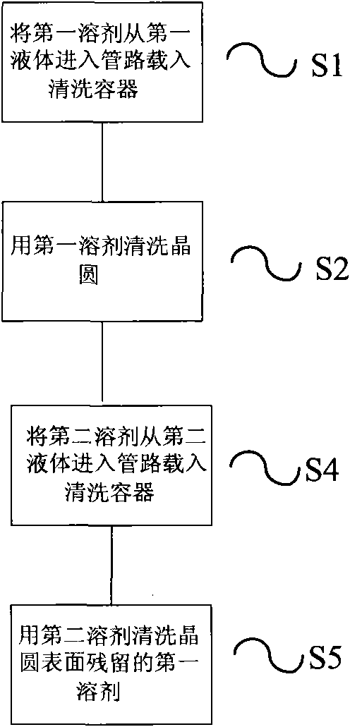
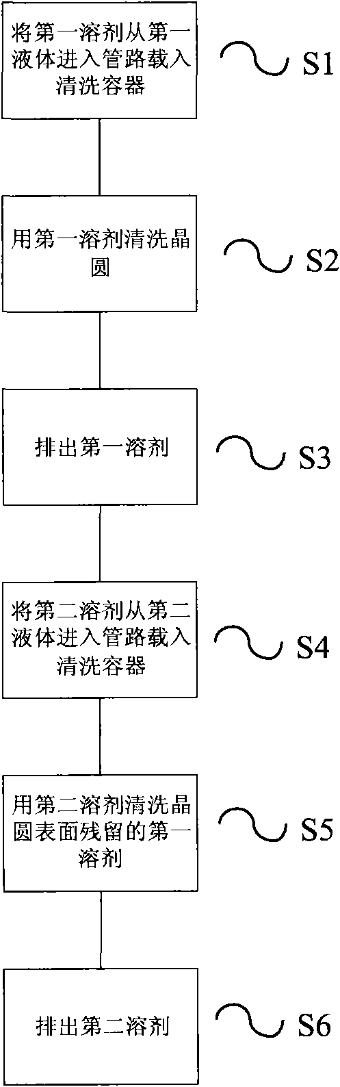
[0042] Such as figure 1As shown, the method includes step S1, inputting the first solvent from the first liquid into the pipeline into the cleaning container, step S2 using the first solvent to clean the wafer, and step S4, inputting the second solvent from the second liquid into the pipeline for cleaning In the container, step S5 uses the second solvent to clean the first solvent on the surface of the wafer. When a failure occurs and the wafer cannot be taken out from the cleaning container, use the second solvent to clean the first solvent on the surface of the wafer to avoid corrosive effects on the wafer. The solvent corrodes the wafer and produces wafer waste, which improves the economy of the wafer cleaning process.

[0043] In order to completely remove the first solvent from the wafer surface, a preferred solution is that the second solvent can dissolve the first solvent. In this way, after the second solvent is input into the cleaning container, the container is sti...

Embodiment 2

[0051] This embodiment provides a cleaning device using the wafer cleaning method in Embodiment 1.

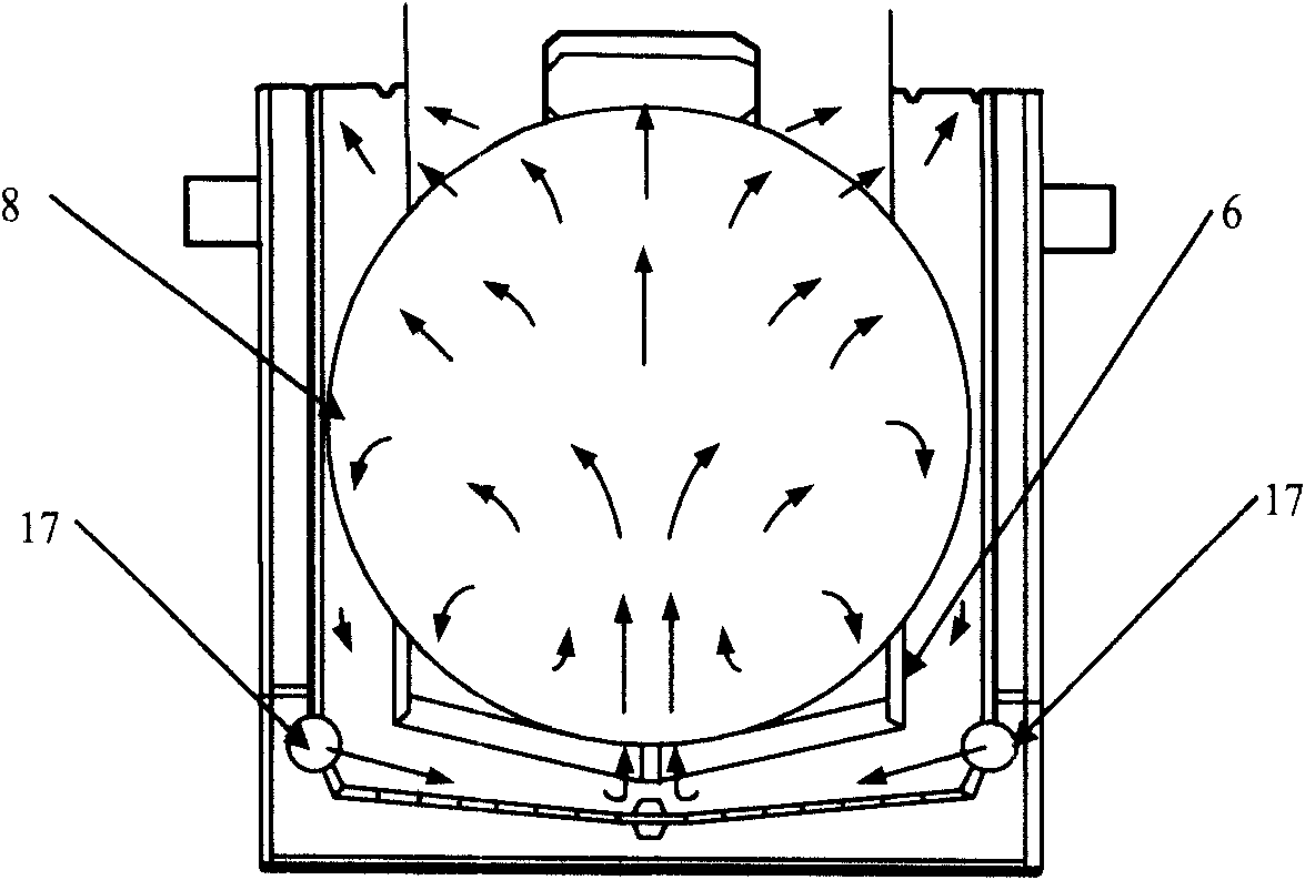
[0052] Such as Figure 4 As shown, this embodiment provides a wafer cleaning device. The cleaning container 7 is provided with a first liquid inlet pipeline 1 for introducing a first solvent, and a second liquid inlet pipeline 2 for introducing a second solvent. By assembling the second liquid into the pipeline 2, providing the passage for the second solvent to enter the cleaning container, the first solvent that remains on the surface of the wafer 8 from the first liquid into the pipeline 1 can be eluted, thereby avoiding the long-term use of the first solvent. The wafer is corroded by contact with the wafer for a long time, thereby improving the economy of the wafer cleaning process and the process adaptability under abnormal working conditions.

[0053] More specifically, the cleaning device includes a cleaning container 7 whose main body is hollow. In the normal use state...


PUM


Abstract

The invention provides a wafer cleaning method, which comprises the following steps: feeding a first solvent into a cleaning container to clean the wafer, and then feeding a second solvent into the cleaning container to clean the first solvent left on the surface of the wafer. A cleaning device using the cleaning method comprises the cleaning container which is provided with a first liquid inlet pipeline and a second liquid inlet pipeline. The first solvent is fed into the cleaning container from the first liquid inlet pipeline, and the second solvent is fed into the cleaning container from the second liquid inlet pipeline. The cleaning device uses the second solvent to clean the first solvent on the surface of the wafer to avoid the long time contact of the first solvent which has corrosion action to the wafer and the wafer, thereby avoiding generation of wafer rejection caused by the corrosion of the wafer by the first solvent, and improving the economy of wafer cleaning technology.

Description

technical field [0001] The invention relates to the technical field of semiconductor manufacturing, in particular to a method for cleaning wafers and a wafer cleaning device using the method. Background technique [0002] The importance of wafer cleaning to the semiconductor industry has attracted people's attention very early, because the residue on the wafer surface will seriously affect the performance, reliability and yield of devices in the subsequent manufacturing process. [0003] Wafer cleaning can be divided into physical cleaning and chemical cleaning, and chemical cleaning includes liquid phase cleaning and gas phase cleaning. Among them, liquid phase cleaning has always occupied a dominant position in the cleaning technology due to many options available, cheap and safe, good selectivity, high cleaning ability and many other advantages. [0004] Regarding the wafer cleaning method, Chinese Patent Application No. 200510000354.3 discloses a wafer cleaning method u...

Claims


Application Information

Patent Timeline
IPC IPC(8): H01L21/00H01L21/02H01L21/306B08B3/08G03F7/30G03F7/42
Inventor 杜亮王福顺谢志勇齐峰
Owner SEMICONDUCTOR MANUFACTURING INTERNATIONAL (BEIJING) CORP
Why Eureka
Try Eureka