Method for reducing defects in memory cell capacitor
A technology of capacitor structure and recessed area, which is applied in the direction of capacitors, electric solid devices, circuits, etc., can solve the problems of complex manufacturing process and structure, difficult to manufacture, etc., and achieve the effect of increasing output
- Summary
- Abstract
- Description
- Claims
- Application Information
AI Technical Summary
Problems solved by technology
Method used
Image

Examples
Embodiment Construction
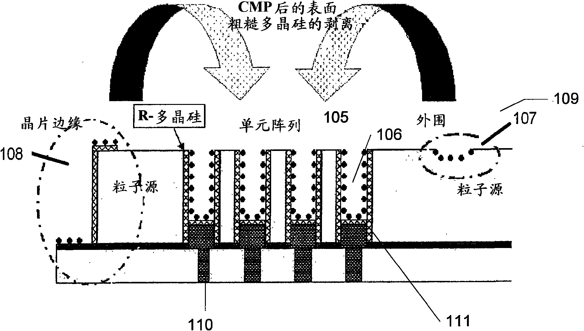
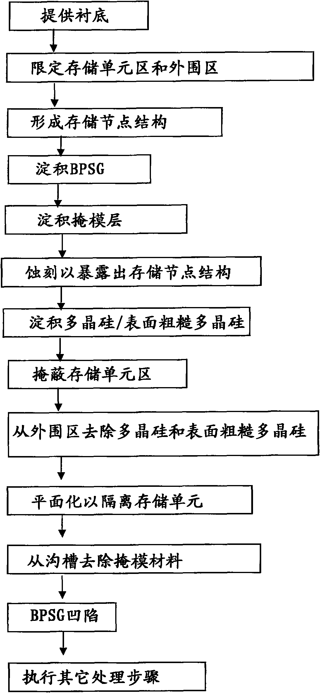
[0017] According to the present invention, an integrated circuit and its processing technology for semiconductor device manufacture are provided. By way of example, the present invention provides a method of fabricating a capacitor for a dynamic random access memory device commonly referred to as a DRAM. It should be recognized, however, that the scope of the invention is much broader. For example, the invention is applicable to microprocessor devices, memory devices, application specific integrated circuit devices, and others.
[0018] A method of fabricating an integrated circuit device can be summarized as follows:
[0019] 1. Provide semiconductor substrates, such as silicon wafers, with a size of 300 mm or more;
[0020] 2. providing a surface region on said semiconductor substrate;
[0021] 3. forming a dielectric layer overlying said surface region;
[0022] 4. planarizing the dielectric layer;
[0023] 5. defining a capacitor region and a peripheral region having ...
PUM
 Abstract
Description
Claims
Application Information
 - R&D
- Intellectual Property
- Life Sciences
- Materials
- Tech Scout
- Unparalleled Data Quality
- Higher Quality Content
- 60% Fewer Hallucinations
Browse by: Latest US Patents, China's latest patents, Technical Efficacy Thesaurus, Application Domain, Technology Topic, Popular Technical Reports.
© 2025 PatSnap. All rights reserved.Legal|Privacy policy|Modern Slavery Act Transparency Statement|Sitemap|About US| Contact US: help@patsnap.com