Electrical connection for semiconductor structures, method for the production thereof, and use of such a connection in a luminous element

A technology of electrical connection structure and conductor structure, applied in the direction of semiconductor devices, semiconductor devices of light-emitting elements, electrical components, etc., can solve problems such as difficulties, achieve good heat dissipation and ensure uniform distribution

Inactive Publication Date: 2010-02-10
诺克特龙金融控股有限公司
View PDF0 Cites 3 Cited by
  • Summary
  • Abstract
  • Description
  • Claims
  • Application Information

AI Technical Summary

Problems solved by technology

[0005] It is more difficult if multiple individual semiconductor structures or LED chips arranged in a certain geometric shape must be mated to each other, for example to be connected in series or in parallel

Method used


Image

  • Electrical connection for semiconductor structures, method for the production thereof, and use of such a connection in a luminous element
  • Electrical connection for semiconductor structures, method for the production thereof, and use of such a connection in a luminous element
  • Electrical connection for semiconductor structures, method for the production thereof, and use of such a connection in a luminous element

Examples


Embodiment Construction

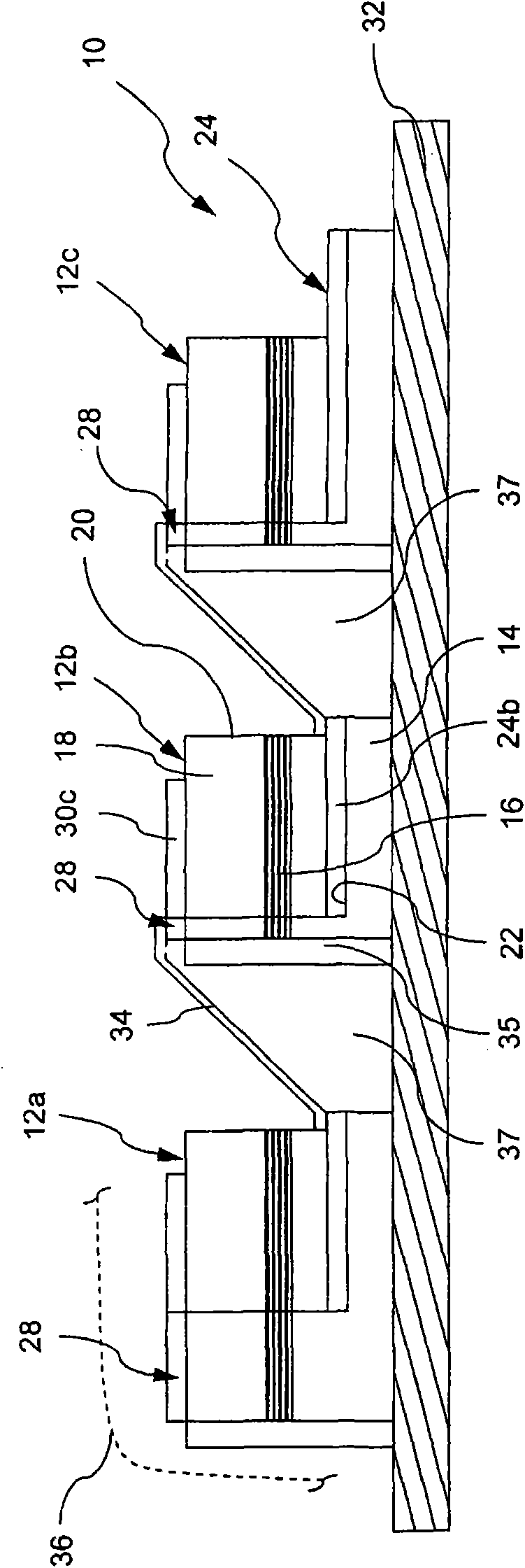
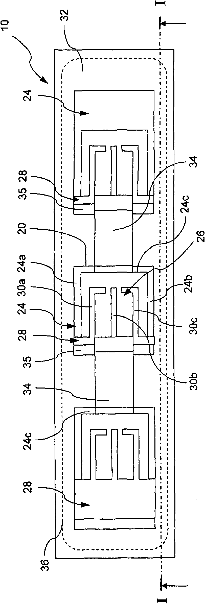
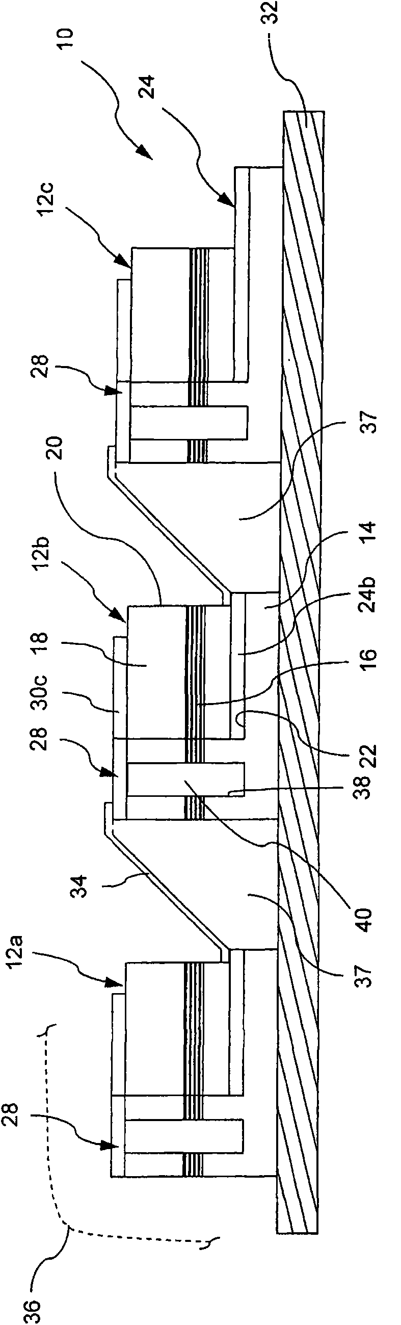
[0033] exist figure 1 and figure 2 In the figure, a light-emitting unit is designated as a whole by the reference number 10, which comprises three semiconductor structures 12a, 12b, 12c. Each semiconductor structure is constructed of three layers, which are only described in the following figure 1 The semiconductor structure 12b arranged in the middle is used as an example for illustration.

[0034] exist figure 1 The lower layer 14 is an n-type layer and is made of, for example, n-GaN or n-InGaN.

[0035] The middle layer 16 is an MQW layer, and MQW is the abbreviation of "Multiplc Quantum Well (Multiple Quantum Well)". MQW material has a superlattice The superlattice has an electronic band structure that varies according to the superlattice structure and correspondingly emits light at different wavelengths. The spectrum of the radiation emitted by the pn-type semiconductor structure 12 can be influenced by the selection of the MQW layer.

[0036] The upper layer 18 ...


PUM

PropertyMeasurementUnit
Areaaaaaaaaaaa
Thicknessaaaaaaaaaa

Abstract

The invention relates to a method for electrically contacting an arrangement of a plurality of semiconductor structures comprising contact regions therefor and emitting electromagnetic radiation whena voltage is applied thereto. According to said method, a viscous, hardenable material is applied to the arrangement of a plurality of semiconductor structures and hardened to form a material web. Theinvention also relates to a luminous element comprising a plurality of semiconductor structures (12) which are interconnected by means of an electrical contacting element (34) and emit visible electromagnetic radiation when a voltage is applied thereto. The electrical contacting element (34) at least partially comprises at least one material web (34) obtained by hardening a material which is viscous in its basic state.

Description

technical field [0001] The invention relates to an electrical connection structure for a semiconductor structure, a manufacturing method of the electrical connection structure and its application in a light emitting unit. Background technique [0002] Generally, a semiconductor structure used in a light emitting device is manufactured from an EPI wafer (Wafer), in other words, a wafer cut out from a semiconductor single crystal. The semiconductor structure is formed on the EPI wafer using photolithographic and / or dry etching methods. To form a light-emitting unit, the semiconductor structures constructed in this way are cut out of the wafer as individual LED chips and mounted as individual LED chips on a carrier substrate / carrier substrate. [0003] Here, each LED chip must be specially bonded for the manufacture of the electrical connection structure. [0004] The "bonding wire" used here is extremely thin and fragile, so the LED chip must be packaged for protection immed...

Claims


Application Information

Patent Timeline
IPC IPC(8): H01L25/075H01L33/00F21K99/00H01L33/38H01L33/62H01L33/64
CPCH01L2924/0002H01L33/38F21K9/00F21V3/04H01L33/647H01L33/62H01L25/0753H01L27/153Y10T29/49117H01L2924/00
Inventor G·迪亚曼蒂迪斯
Owner 诺克特龙金融控股有限公司
Why Eureka
Try Eureka