
Aplanatism pentahedral visual detecting process

A technology of visual appearance and light source, applied in the field of optical devices and visual inspection systems, can solve the problems of inability to eliminate optical path difference deformation and complex system.

Inactive Publication Date: 2010-02-17
CHINTOP MICROELECTRONICS SHANGHAI +2
View PDF0 Cites 17 Cited by
  • Summary
  • Abstract
  • Description
  • Claims
  • Application Information

AI Technical Summary

Problems solved by technology

Existing technology can only reach the quasi-3D level when performing five-sided inspection, or even if a 3D image is obtained, the system is extremely complicated, and the deformation caused by the optical path difference cannot be eliminated

Method used


Image

  • Aplanatism pentahedral visual detecting process
  • Aplanatism pentahedral visual detecting process
  • Aplanatism pentahedral visual detecting process

Examples


Embodiment Construction

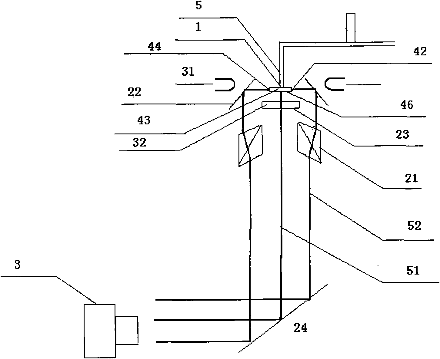
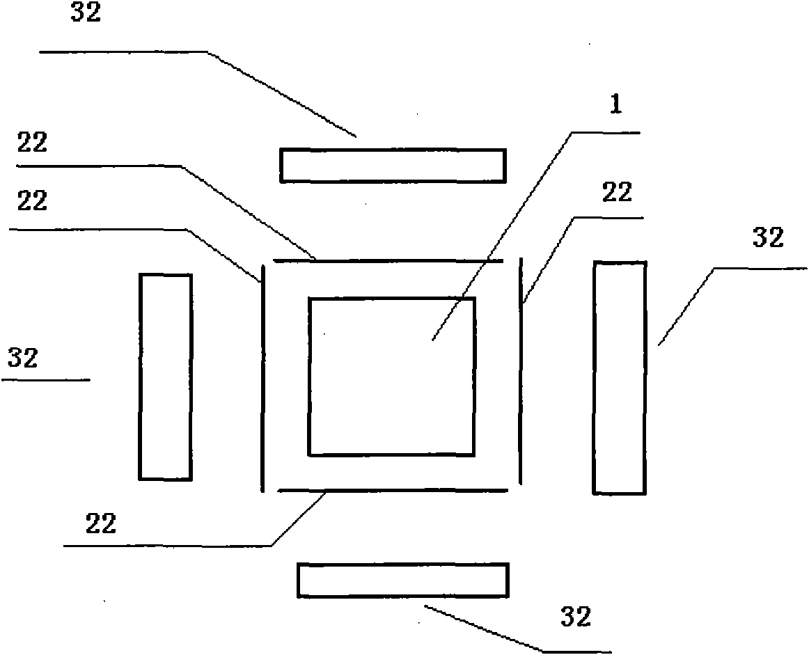
[0016] figure 1 The example shown is that the electronic component 1 is sent by the suction nozzle to the inspection station through the conveying device. The frontal image 46 passes through the optical path 51 generated by the low-angle shadowless light source 31 , passes through the polarizer 23 , and then enters the camera 1 after being reflected by the side-view mirror 24 . At least one lateral side image 42, 43, 44, 45 generates an optical path 52 after the light source is provided by the side spotlight 32, is reflected by the coated glass 22, enters the polarization beam splitter prism 21, and enters the camera 3 after being reflected by the side-view mirror 24 .

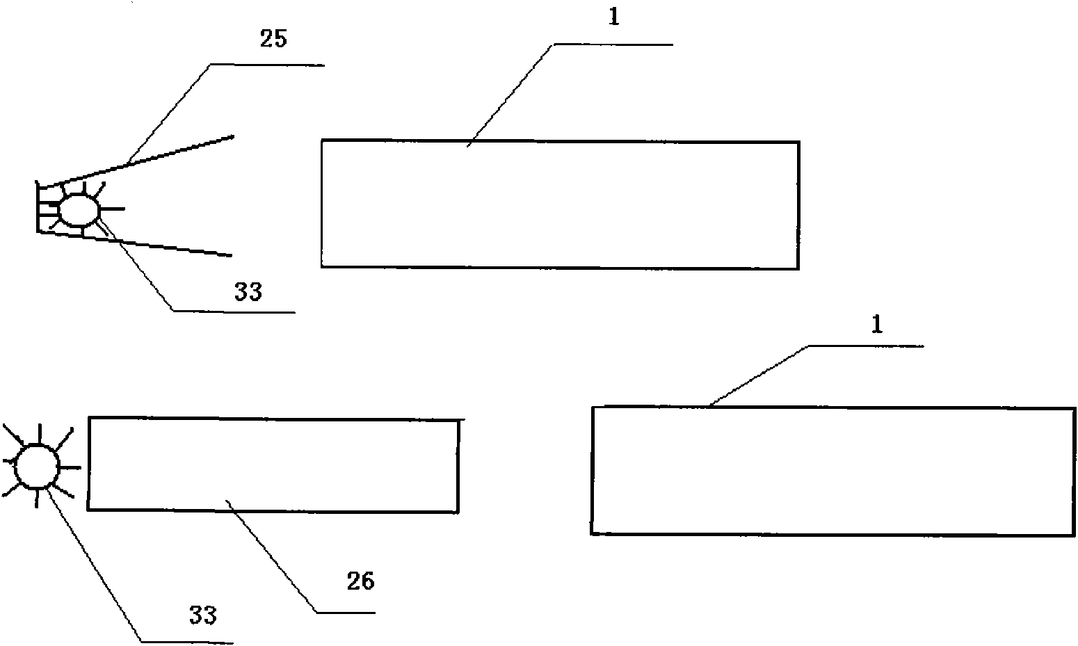
[0017] Figure 5 In the example shown, the electronic component 1 is put into the workbench 4 by the suction nozzle, and then clamped by the clamp 6 after being put into it. Turning to the bottom of the camera 2, the light source 33 provides a light source, and the top surface image 41 is taken by it. The ...


PUM


Abstract

The invention relates to a new visual detecting process which can carry out the visual appearance detection of an IC component 1. The process mainly comprises the following steps: 1. improving an image by the characteristics of the polarization and refraction of a polarized beam-splitting prism 21; 2. scaling a viewing field according to the size of the component by the adjustment of a reflectingsystem; 3. using one group of light sources 31 and the other group of light sources 32 to illuminate a detecting surface 41, a detecting surface 42, a detecting surface 43, a detecting surface 44 anda detecting surface 45 with different requirements; and 4. imaging by using single surface reflecting properties of film plating glass 22. The polarized beam-splitting prism can polarize an optical path, achieve the function of improving an image and can enable the different detecting surface 41, the detecting surface 42, the detecting surface 43, the detecting surface 44 and the detecting surface45 to have the same visual optical path with a center image 46, thereby realizing multi-surface image optimization by the relatively simple and convenient process.

Description

technical field [0001] The present invention relates to optical devices and visual inspection systems incorporating such systems. The present invention is mainly applied to (but not limited to) visual inspection of quad flat no-lead devices (QFN) and the like. It can detect (but not limited to) the appearance of electronic components QFN, pins, copper contamination, pin center distance, burrs, substrate surface flatness, etc. Background technique [0002] For leadless packages including QFN in electronic components, factors such as pad quality, copper burrs and flatness directly affect the yield rate and production efficiency in subsequent processes. Including welding quality, electrical properties and so on. Therefore, visual appearance inspection plays an extremely important role in the taping process of electronic components. Existing technologies can only reach the quasi-3D level when performing five-sided detection, or even if 3D images are obtained, the system is ex...

Claims


Application Information

Patent Timeline
IPC IPC(8): G01B11/00G01B11/30G01B11/02G01N21/84G01N21/88G02B27/28
Inventor 张健欣胡俊韡
Owner CHINTOP MICROELECTRONICS SHANGHAI
Learn More