Plasma-processing device and method of manufacturing adhesion-preventing member

A plasma and processing device technology, applied in the fields of plasma, semiconductor/solid-state device manufacturing, electrical components, etc., can solve problems such as the impact of manufacturing yields, and achieve the effects of reducing manufacturing costs, reducing metal pollution, and improving manufacturing yields

Active Publication Date: 2010-02-17
ULVAC INC
View PDF3 Cites 3 Cited by
  • Summary
  • Abstract
  • Description
  • Claims
  • Application Information

AI Technical Summary

Problems solved by technology

Therefore, when the degree of contamination becomes high, the characteristics of the devices formed on the substrate will change, which will affect the manufacturing yield.

Method used


Image

  • Plasma-processing device and method of manufacturing adhesion-preventing member
  • Plasma-processing device and method of manufacturing adhesion-preventing member
  • Plasma-processing device and method of manufacturing adhesion-preventing member

Examples


no. 1 approach

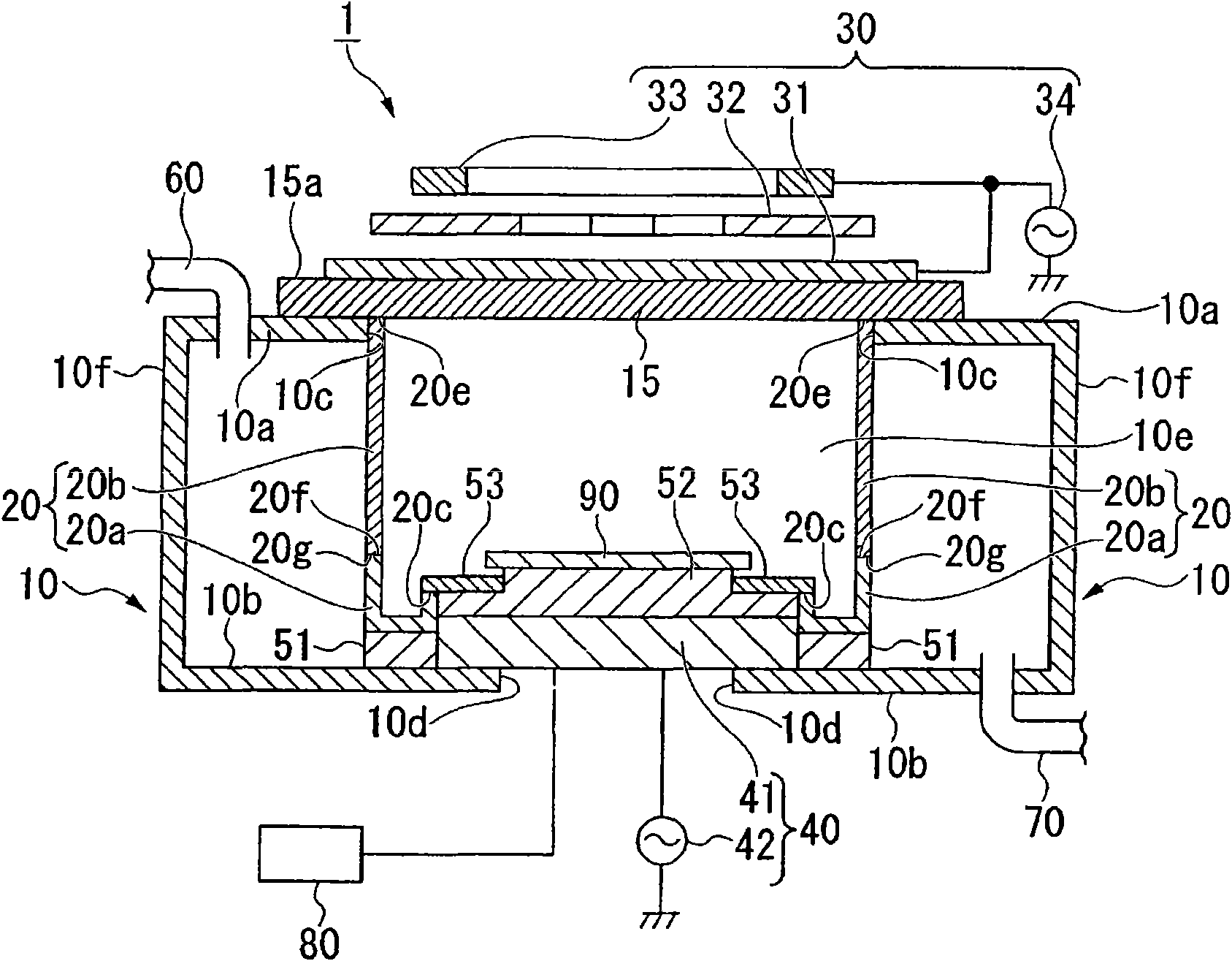
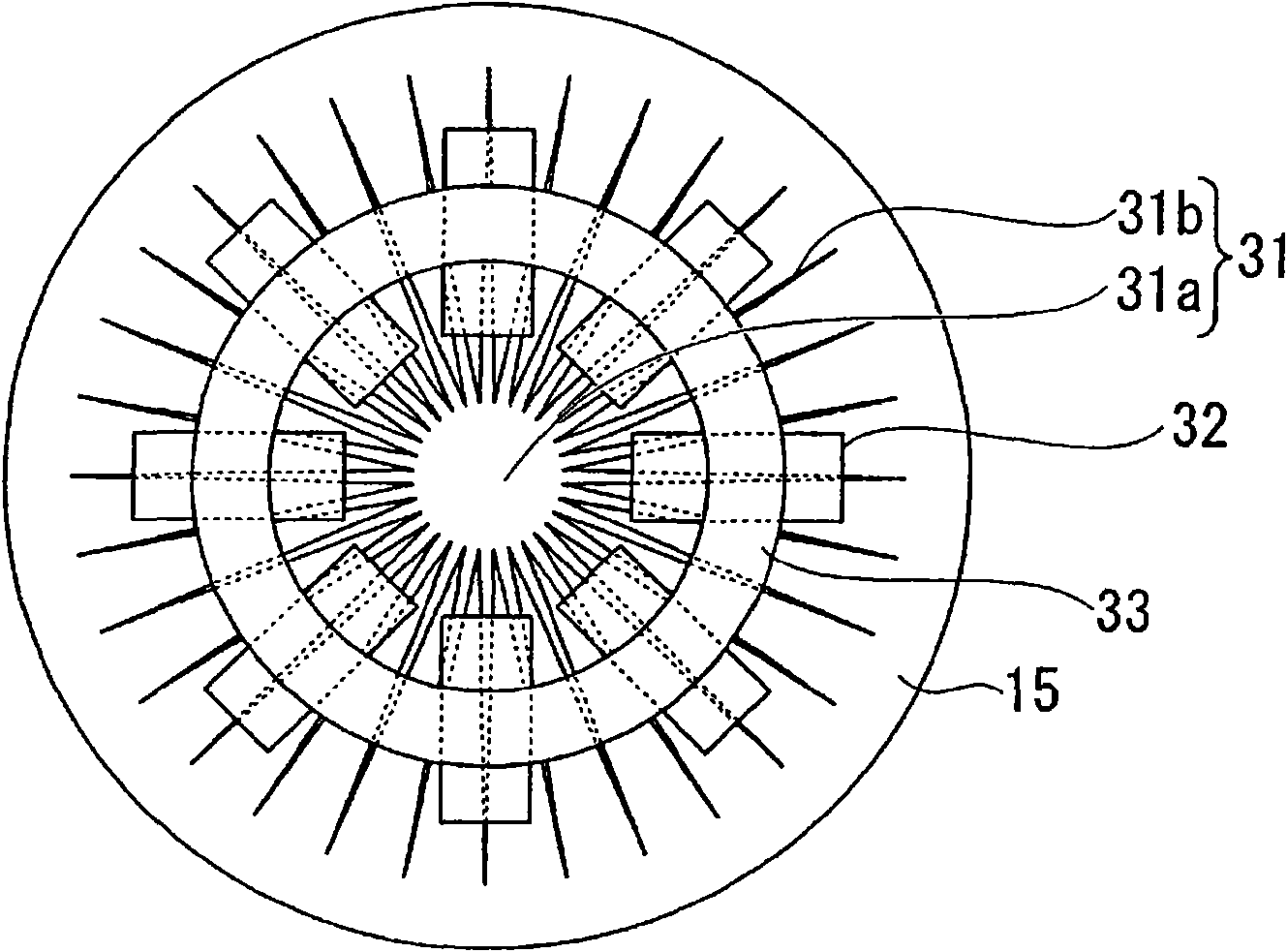
[0052] figure 1 It is a schematic block diagram of the etching apparatus (plasma processing apparatus) 1 of this invention. The etching apparatus 1 includes a processing chamber 10, an anti-adhesion member 20, a plasma generation device 30, a bias voltage generation device 40, a first quartz plate 15, a heating device 51, a support member 52, a second quartz plate 53, an air intake device 60, Exhaust device 70 and cooling device 80 . The plasma generating apparatus 30 has a first electrode 31 , a permanent magnet 32 ​​, an antenna 33 and a first high-frequency power source 34 . The bias voltage generating device has a second electrode 41 and a second high frequency power source 42 .

[0053] The processing chamber 10 is formed in a cylindrical shape, has an opening 10c in the top wall 10a, and has an opening 10d in the bottom wall 10b. The first quartz plate 15 is placed outside the ceiling wall 10a of the processing chamber 10 so as to cover the opening 10c. The first ele...


PUM

PropertyMeasurementUnit
thicknessaaaaaaaaaa
thicknessaaaaaaaaaa
surface roughnessaaaaaaaaaa

Abstract

A plasma-processing device comprises a constituent member which performs plasma- processing of a noble metal material and a ferroelectric material on a substrate to be processed and is exposed to plasma while being heated. The constituent member is made of an aluminum alloy having an aluminum purity of 99% or higher.

Description

technical field [0001] The present invention relates to a plasma processing apparatus and a method for manufacturing an anti-adhesion member. [0002] This application takes Japanese Patent Application No. 2007-132631 and Japanese Patent Application No. 2007-146753 as basic applications, and the contents thereof are incorporated. Background technique [0003] The etching process using a plasma processing apparatus is performed by making the reaction gas excited into a plasma state collide with the structure formed on the substrate. Due to the etching process, products such as particles of the structure combined with the reaction gas or simple particles of the structure fly out from the structure. Therefore, in order to prevent the products from adhering to the wall of the processing chamber, the wall of the processing chamber and the substrate An anti-adhesion plate is arranged in between. [0004] As a material of an anti-adhesion plate, the material etc. which processed ...

Claims


Application Information

Patent Timeline
Patent Type & Authority Applications(China)
IPC IPC(8): H01L21/3065H05H1/46
CPCH01J37/32467H01J37/32568H01J37/32009H01J37/321H01L21/3065H05H1/46
Inventor 小风丰植田昌久远藤光广邹红罡宫崎俊也酒田现示中村敏幸
Owner ULVAC INC
Why Eureka
Try Eureka