Sheet material, method for manufacturing same and product shell
A production method and sheet technology, which are applied in the direction of layered products, chemical instruments and methods, synthetic resin layered products, etc., can solve the problems of lack of three-dimensional effect, single color of metal effect, etc.
- Summary
- Abstract
- Description
- Claims
- Application Information
AI Technical Summary
Problems solved by technology
Method used
Image
Examples
Embodiment 1
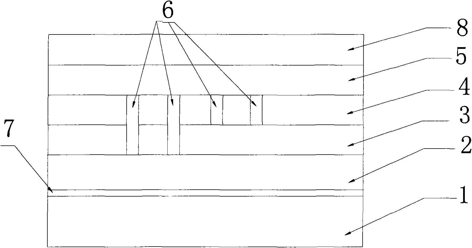
[0064] How to make plastic sheet
[0065] (1) Select an ABS base layer 1 with a thickness of 3mm, and bake it at 80°C for 8 hours to remove the stress of the base layer 1;
[0066] (2) Clean and remove impurities on both surfaces of the base layer 1 whose stress has been removed in step (1);
[0067] (3) For the base layer 1 cleaned in step (2), wipe the oil agent with an alkaline solvent, wherein the degreasing agent cannot affect the surface effect of the base layer.
[0068] (4) The surface of the base layer 1 after step (3) is degreased is activated by various activation techniques known to those skilled in the art, mainly roughening, sensitization, and three steps of activation, so that the surface of the base layer 1 forms a metal catalyst center.
[0069] (5) To the base layer 1 after step (4) activation, adopt electroplating technology known to those skilled in the art, plate one layer of chemical nickel film layer 7, wherein, electroplating condition is: nickel sulf...
Embodiment 2
[0081] How to make plastic sheet
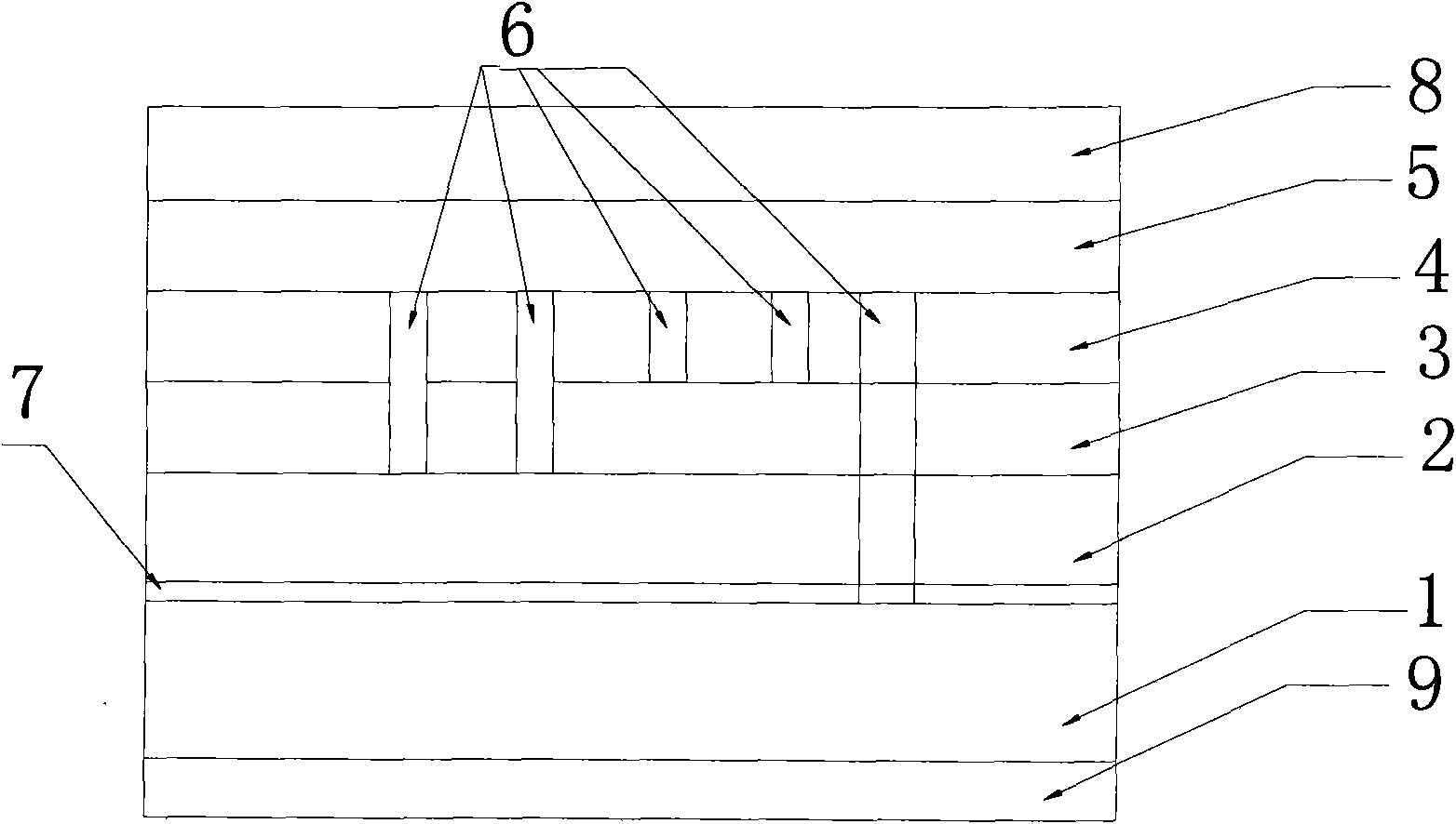
[0082] (1) According to the same steps and methods as steps (1) to (9) of Example 1, a plastic sheet is made. The difference is that a layer of anti-plating ink is coated on the second surface of the base layer during pre-plating treatment.
[0083] (2) Dry the plastic sheet that has completed step (1) to obtain a plastic sheet plated with four metal layers of nickel, copper, tin, and chromium. Use EPYAG25 laser equipment with a current of 21A to engrave the desired pattern. 6. Adjust the depth of laser engraving by adjusting the current of the laser equipment. It is better to just expose part of the copper layer 2, part of the tin layer 3 and part of the base layer 1.
[0084] (3) Prepare the DSMT100P series metal paint 1, spray it on the reverse side of the material obtained in step (2) to obtain a film layer 9, and then bake it at 70°C for 2 hours, and the film thickness is 15 μm.
[0085](4) Spray a layer of polyurethane colored paint 5...
PUM
| Property | Measurement | Unit |
|---|---|---|
| Thickness | aaaaa | aaaaa |
| Thickness | aaaaa | aaaaa |
| Thickness | aaaaa | aaaaa |
Abstract
Description
Claims
Application Information
 - R&D
- Intellectual Property
- Life Sciences
- Materials
- Tech Scout
- Unparalleled Data Quality
- Higher Quality Content
- 60% Fewer Hallucinations
Browse by: Latest US Patents, China's latest patents, Technical Efficacy Thesaurus, Application Domain, Technology Topic, Popular Technical Reports.
© 2025 PatSnap. All rights reserved.Legal|Privacy policy|Modern Slavery Act Transparency Statement|Sitemap|About US| Contact US: help@patsnap.com


