
Eureka
For R&D, Eureka makes reading and utilizing patents & technical documents easy.
Eureka AIR
Designed for self-driven R&D workflows. Generate viable solutions, solve complex R&D challenges, empower your innovation with AI.

Eureka Materials
Designed for material experts only. Revolutionize your material R&D, from search, analyze, to developing new materials.

TechResearch
Generate reliable direction feasibility study reports for your R&D in just a few steps.

TechSeek
Discover and master advanced knowledge NOW. Basics, ideas, possibilities, all at once.

TechMind
As an expert in R&D Theories, TechMind can generates customized viable solutions instantly.

TechRisk
Analyze your overall solution with one click, know your potential R&D risks in advance.

TechMonitor
Get weekly tech updates, stay abreast of the latest tech innovations and key insights.
LED packaging module and preparation method thereof
A technology of LED packaging and LED chips, applied in lighting devices, lighting and heating equipment, components of lighting devices, etc., can solve the problems of poor thermal conductivity, difficulty in taking into account thermal conductivity and firmness, and poor firmness.
- Summary
- Abstract
- Description
- Claims
- Application Information
AI Technical Summary
Problems solved by technology
Method used
Image

Examples
Embodiment Construction
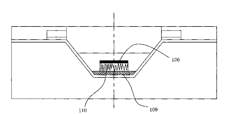
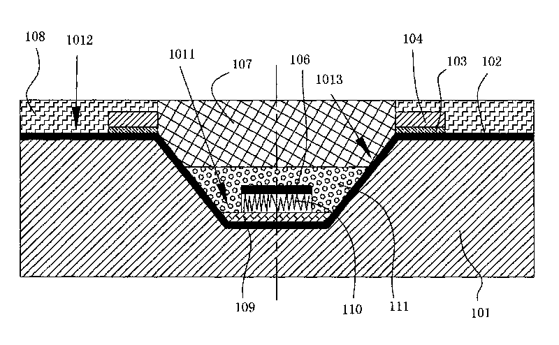
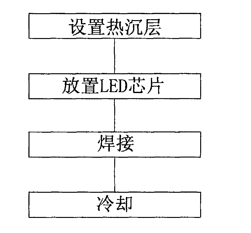
[0022] The present invention will be described in further detail below in conjunction with the accompanying drawings. refer to figure 1 , figure 2 , the first embodiment of the present invention is an LED packaging module, including a substrate 101 and an LED chip 110; the substrate 101 is an AlSi alloy material, wherein the content of Al is 30%-95%, and the content of Si is 5%- 70%; the substrate 101 has a crystal-bonding surface 1011 and a wiring surface 1012, the crystal-bonding surface 1011 is arranged parallel to the wiring surface 1012, the height of the crystal-bonding surface 1011 is lower than the wiring surface 1012, and the A reflective surface 1013 is provided between the crystal bonding surface 1011 and the wiring surface 1012; a reflective film 102 is provided on the surface of the crystal bonding surface 1011, the wiring surface 1012, and the reflective surface 1013, and the reflective The film structure of the film 102 is Ni-Ag-Ni; the thickness of each laye...
PUM
 Abstract
Description
Claims
Application Information
 - R&D Engineer
- R&D Manager
- IP Professional
- Industry Leading Data Capabilities
- Powerful AI technology
- Patent DNA Extraction
Browse by: Latest US Patents, China's latest patents, Technical Efficacy Thesaurus, Application Domain, Technology Topic, Popular Technical Reports.
© 2024 PatSnap. All rights reserved.Legal|Privacy policy|Modern Slavery Act Transparency Statement|Sitemap|About US| Contact US: help@patsnap.com