Liquid crystal display panel and manufacturing method thereof

A technology for liquid crystal display panels and manufacturing methods, applied in the fields of nonlinear optics, instruments, optics, etc., can solve the problems of height difference between the peripheral area of ​​the panel and the central area of ​​the panel, uneven display of peripheral images, and different gaps between liquid crystal display panels, etc., to achieve The effect of improving the utilization rate

Inactive Publication Date: 2010-04-28
CENTURY DISPLAY (SHENZHEN) CO LTD
View PDF0 Cites 38 Cited by
  • Summary
  • Abstract
  • Description
  • Claims
  • Application Information

AI Technical Summary

Problems solved by technology

[0006] The invention provides a liquid crystal display panel, which can solve the problem in the prior art that when two substrates are bonded together using sealant and conductive particles, because the particle size of the conductive particles is larger than the size diameter of the spacer, the peripheral area of ​​the panel and the panel The gap in the central area produces a height difference,

Method used


Image

  • Liquid crystal display panel and manufacturing method thereof
  • Liquid crystal display panel and manufacturing method thereof
  • Liquid crystal display panel and manufacturing method thereof

Examples


no. 1 example

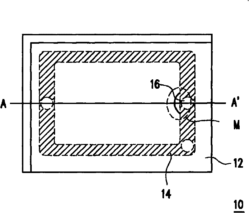
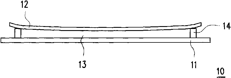
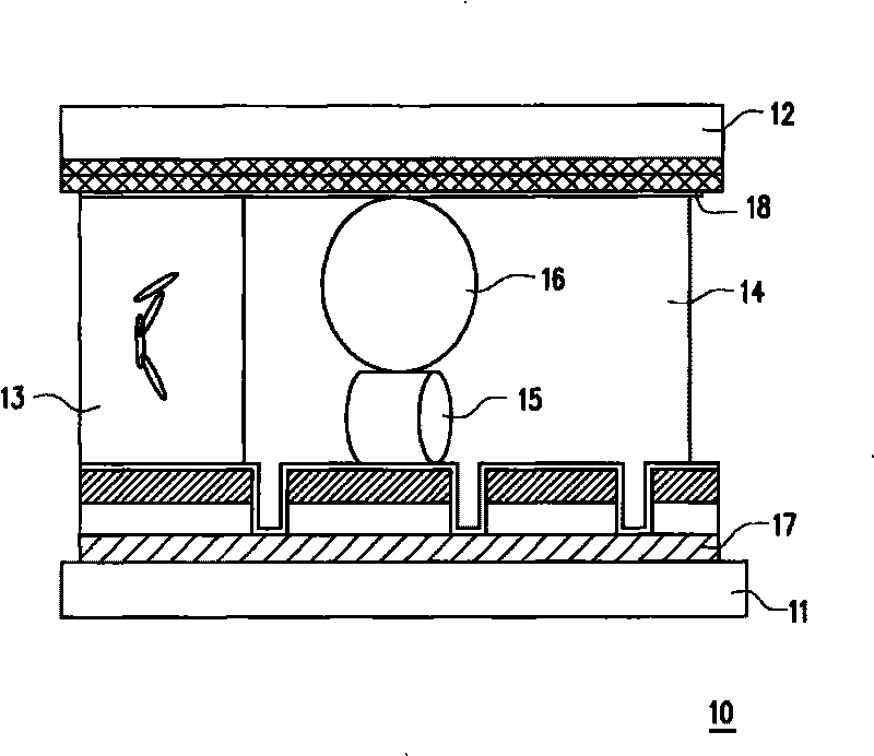
[0039] Figure 4A It is a partial cross-sectional enlarged view of the sealant 34 area of ​​the liquid crystal display panel in the first embodiment of the present invention. see Figure 4A The liquid crystal display panel 20 has a display area 21 and a peripheral area 22 located on the periphery of the display area 21, and the liquid crystal display panel 20 includes a first substrate 31, a second substrate 32, a liquid crystal layer 33, and a sealant 34, wherein the first substrate 31 and The second substrate 32 is, for example, a thin film transistor substrate and a color filter substrate, respectively. The first substrate 31 and the second substrate 32 are arranged opposite to each other at a certain substrate distance D0, the liquid crystal layer 33 is arranged between the first substrate 31 and the second substrate 32, and the sealant 34 is sandwiched between the first substrate 31 and the second substrate 32 Between, around the liquid crystal layer 33 to surround and ...

no. 2 example

[0060] Figure 6 It is a partial cross-sectional enlarged view of the frame glue area of ​​the liquid crystal display panel according to the second embodiment of the present invention. Please refer to Figure 6 The liquid crystal display panel 30 of the second embodiment is similar to the first embodiment, except that on the second substrate 32 of the liquid crystal display panel 30 of the present embodiment, the black matrix 41 further provides a second contact hole H2, and the common electrode 42 covers the black The matrix 41 extends to the inner surface of the second contact hole H2 , and the common electrode 42 in the second contact hole H2 is connected to the contact electrode 39 in the first contact hole H1 through the conductive particles 40 .

[0061] Furthermore, the opening position of the second contact hole H2 of the black matrix 41 is set relative to the position of the first contact hole H1. As described in the first embodiment, the diameter and depth of the se...


PUM

PropertyMeasurementUnit
Apertureaaaaaaaaaa
Depthaaaaaaaaaa
Diameteraaaaaaaaaa

Abstract

The invention relates to a liquid crystal display panel and a manufacturing method thereof. The liquid crystal display panel comprises a first substrate, a second substrate, a frame glue and a liquid crystal layer positioned between the first substrate and the second substrate; the peripheral region of the first substrate is provided with a first metal wiring, a dielectric layer covering the first metal wiring and a contact electrode, wherein, the dielectric layer is provided with a contact hole, and the contact electrode covers on the inner surface of the dielectric layer and the contact hole; the second substrate is arranged corresponding to the first substrate; the frame glue is arranged between the peripheral regions of the first substrate and the second substrate, and comprises conducting particles which are arranged in the contact hole and are contacted with the contact electrode, so that the liquid crystal display panel of the invention can avoid Mura phenomenon of the peripheral picture display caused by the condition that the gap of peripheral region is higher than the gap of the central region.

Description

【Technical field】 [0001] The present invention relates to a display panel and a manufacturing method thereof, in particular to a liquid crystal display panel and a manufacturing method thereof, which can avoid display unevenness (Mura )The phenomenon. 【Background technique】 [0002] The liquid crystal display panel is the key component of the liquid crystal display device. Its main components usually include two glass substrates, a sealant coated between the two glass substrates, and a space formed by the sealant and the two glass substrates. of liquid crystal molecules. Among the above two glass substrates, one of the substrates has multiple sets of pixel electrodes, which are used to control the rotation angle of liquid crystal molecules according to the input data voltage; the other substrate has color filters, which are used to make the liquid crystal panel display color images . In the prior art, the thin-film transistor substrate and the color filter substrate of th...

Claims


Application Information

Patent Timeline
IPC IPC(8): G02F1/1333G02F1/1339G02F1/1362G02F1/1368
Inventor 李得俊曾迎祥
Owner CENTURY DISPLAY (SHENZHEN) CO LTD
Why Eureka
Try Eureka