Anti-radiation field effect transistor, CMOS integrated circuit and preparation thereof

A technology of field effect transistors and body regions, which is applied in the manufacture of transistors, circuits, semiconductors/solid-state devices, etc., and can solve problems such as increased power consumption, poor resistance to total dose effects, and increased off-state current.

Inactive Publication Date: 2010-05-12
SEMICONDUCTOR MANUFACTURING INTERNATIONAL (BEIJING) CORP +1
View PDF0 Cites 24 Cited by
  • Summary
  • Abstract
  • Description
  • Claims
  • Application Information

AI Technical Summary

Problems solved by technology

However, due to the existence of the SOI substrate, its inherently thicker buried oxide layer will capture holes when irradiated by the space radiation source, causing the back gate transistor to be turned on, thereby causing an increase in the off-state current and increasing power consumption. At the same time, it may also affect the front gate threshold,

Method used


Image

  • Anti-radiation field effect transistor, CMOS integrated circuit and preparation thereof
  • Anti-radiation field effect transistor, CMOS integrated circuit and preparation thereof
  • Anti-radiation field effect transistor, CMOS integrated circuit and preparation thereof

Examples


Embodiment Construction

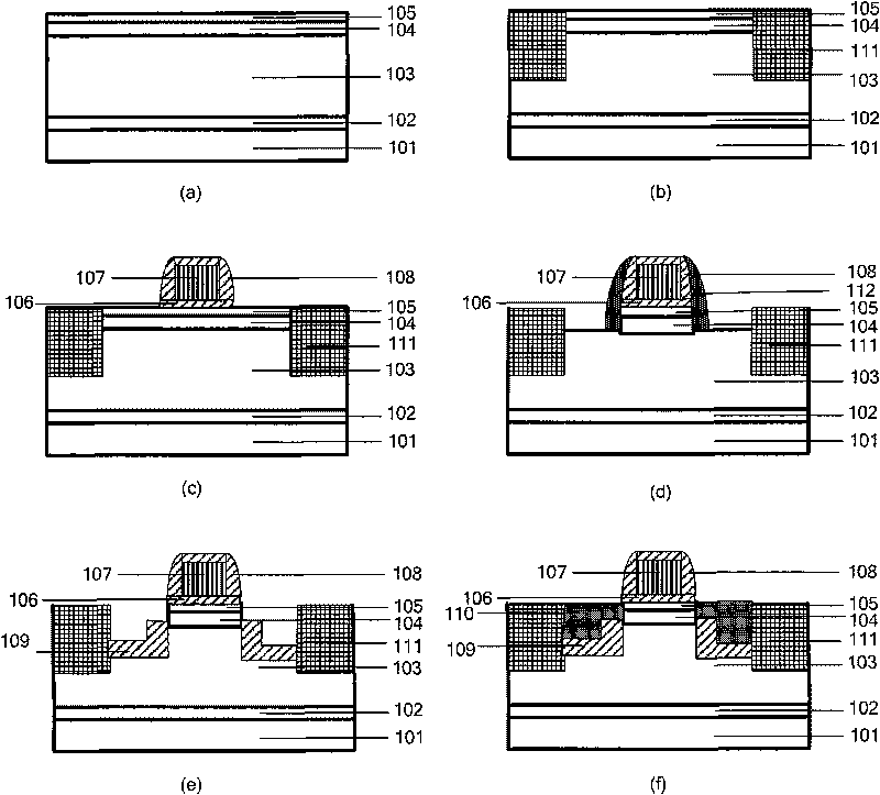
[0029] Attached below figure 2 (a)---(e) further describe in detail the preparation method and process flow of N-type field effect transistor of the present invention:

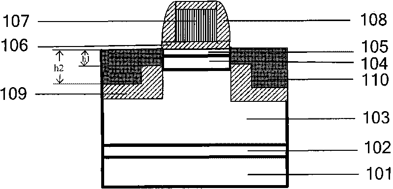
[0030] 1) On the p-type bulk silicon substrate 101, sequentially epitaxially n+ epitaxial layer 102, p well region 103, p+ epitaxial layer 104 and p epitaxial layer 105, such as figure 2 As shown in (a), wherein the thickness of the n+ epitaxial layer 102 is 50-250 nm, the thickness of the p well region 103 is 150-500 nm, the thickness of the p+ epitaxial layer 104 is 20-50 nm, and the thickness of the p epitaxial layer 105 is 10-20 nm ,Such as figure 2 (a) shown.

[0031] 2) Shallow trench isolation (STI) is used to define the active region, and the depth of the STI isolation region 111 is 250-350nm, preferably 300nm, such as figure 2 (b) shown.

[0032] 3) Thermally oxidize the gate oxide layer 106, deposit polysilicon gate material, perform n-type doping implantation on the polysilicon material, act...


PUM

PropertyMeasurementUnit
Thicknessaaaaaaaaaa
Doping concentrationaaaaaaaaaa
Thicknessaaaaaaaaaa

Abstract

The invention discloses an anti-radiation field effect transistor, a CMOS integrated circuit and a preparation method thereof, wherein an N-type field effect transistor is provided with an n+ epitaxial layer between a substrate and a body area; a channel is a p/p+ inverse doped structural layer; a source and a drain are isolated from the body area through an L-shaped insulating layer respectively; the distance from the top surface of the L-shaped insulating layer to the upper surface of the channel is smaller than the thickness of the channel; the corresponding n+ epitaxial layer is changed into a p+ epitaxial layer; and the p/p+ inverse doped structural layer is changed into an n/n+ inverse doped structural layer so as to form a P-type field effect transistor. The transistor not only resists single-particle effects, but also resists total-dose effects. The CMOS integrated circuit formed can fundamentally solve the singleness problem of anti-radiation effects. In addition, the transistor can be prepared based on a bulk-silicon substrate and does not need SOI substrates, thereby having the advantages of reduced cost, simple preparation method, compatibility with conventional CMOS processes and good controllability.

Description

technical field [0001] The invention relates to integrated circuit anti-irradiation technology, in particular to an anti-irradiation quasi-SOI field effect transistor, CMOS integrated circuit and a preparation method thereof. Background technique [0002] The rapid development and wide application of information technology has changed the traditional production, management, management and life style, and has brought a profound impact on all aspects of human society. As we all know, the key to realizing social informatization is all kinds of computers and communication machines, the basis of which is microelectronic products, and the core is silicon-based CMOS integrated circuits. With the development of science and technology, especially the development of space technology, nuclear power and nuclear weapons, the relationship between nuclear radiation environment and electronic technology is getting closer. At present, my country's aerospace technology is developing rapidly....

Claims


Application Information

Patent Timeline
IPC IPC(8): H01L29/78H01L27/092H01L21/336
Inventor 薛守斌黄如张兴
Owner SEMICONDUCTOR MANUFACTURING INTERNATIONAL (BEIJING) CORP
Why Eureka
Try Eureka