High speed image data acquisition and processing card based on Camera Link interface

A data acquisition and processing, high-speed image technology, applied in electrical digital data processing, data processing input/output process, instruments, etc., can solve the problems of limited acquisition speed, poor portability, inconvenient use, etc., to achieve convenient use and maintenance , the collection speed is fast, the effect of easy to upgrade

Inactive Publication Date: 2010-05-19
CHANGCHUN INST OF OPTICS FINE MECHANICS & PHYSICS CHINESE ACAD OF SCI
View PDF0 Cites 29 Cited by
  • Summary
  • Abstract
  • Description
  • Claims
  • Application Information

AI Technical Summary

Problems solved by technology

[0002] As more and more industrial camera manufacturers adopt the standard Camera Link interface protocol, the image acquisition and processing card based on the standard Camera Link interface has been widely demanded, while the traditional image acquisition card has poor portability, fixed interface, and low function. single, inconvenient to use
And a common feature of these products is: they are connected to the PC through PCI slot, USB or Ethernet, and the main image processing program is completed on the PC (Personal Computer), which makes the volume of the system relatively large, and not only costs more high and difficult to maintain
At the same time, the acquisition speed of these traditional image acquisition cards is limited, and it is difficult to achieve the acquisition task of high frame rate cameras

Method used


Image

  • High speed image data acquisition and processing card based on Camera Link interface
  • High speed image data acquisition and processing card based on Camera Link interface
  • High speed image data acquisition and processing card based on Camera Link interface

Examples


Embodiment Construction

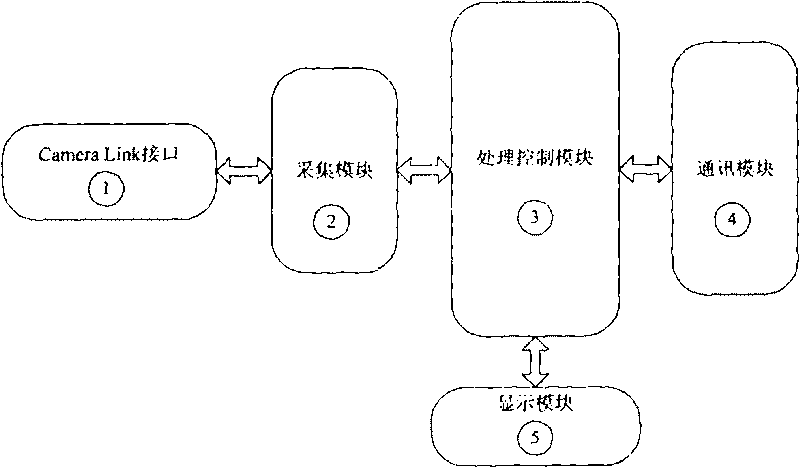
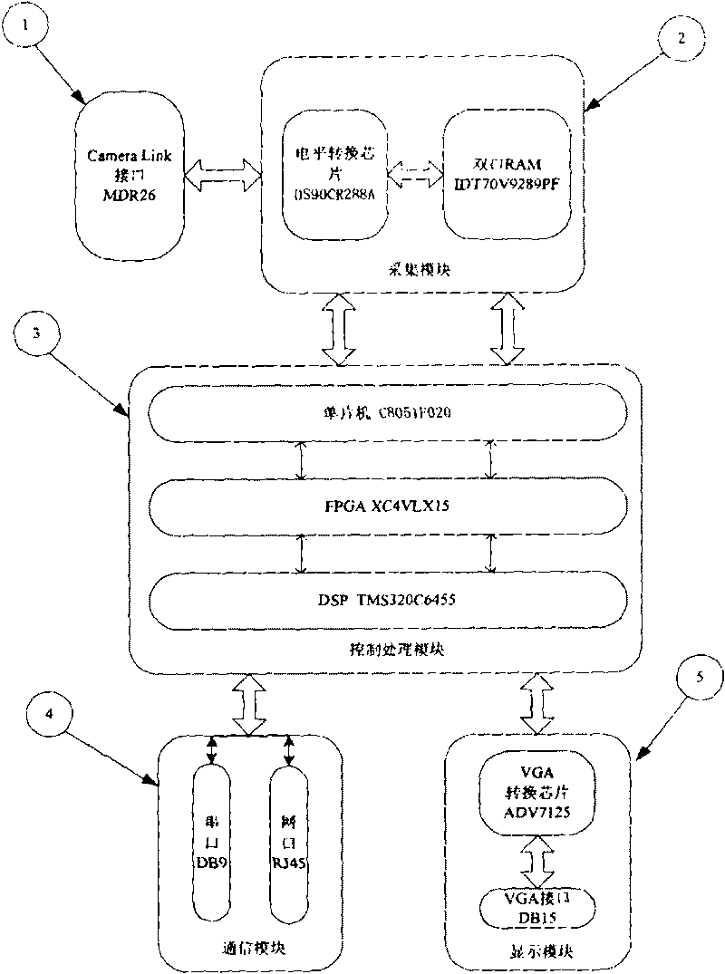
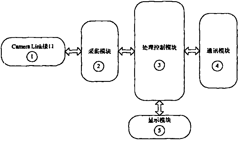
[0024] The previous technical scheme gives the overall technical route. In the specific implementation, different specific components should be used for the five modules. as attached figure 2 As shown, select the corresponding device corresponding to each component, solder and fix it on the printed circuit board, and make a high-speed image data acquisition and processing card. in:

[0025] Camera Link interface connector (MDR 26-Pin Connector): This part is used to import camera data into the device.

[0026] Level conversion chip (DS90CR288A): This part is used to realize the conversion of camera LVDS signal to TTL signal.

[0027] Dual-port RAM (IDT70V9289PF): This component cooperates with FPGA to realize the function of acquisition module.

[0028] Single-chip microcomputer (C8051F020): This component is mainly used to realize the control function in the processing control module.

[0029] Field Programmable Gate Array (XC4VLX15): This component mainly implements the...


PUM


Abstract

The invention relates to a high speed image data acquisition and processing card based on a Camera Link interface, belonging to the field of digital image communication processing. The high speed image data acquisition and processing card comprises a Camera Link interface, an acquisition module, a processing control module, a communication module and a display module; after an opening command of a singlechip is received, data are led into a level switching chip through an external interface camera, a TTL level formed through switching enters a double-port RAM under the control of a programmable gate array to realize acquisition and processing, digital signals are switched into analog signals through a VGA switching chip and then displayed on an external display screen through a VGA interface, and communication with external equipment is realized in real time through a serial port and a network port. The high speed image data acquisition and processing card has multiple functions, high integration density, compact structure, high acquisition speed and convenient use and maintenance, and is also convenient to upgrade, maintain and secondarily develop.

Description

Technical field: [0001] The invention belongs to the field of digital image communication processing, and mainly relates to an electronic device for collecting and processing image data of a current general standard CameraLink interface camera. Background technique: [0002] As more and more industrial camera manufacturers adopt the standard Camera Link interface protocol, the image acquisition and processing card based on the standard Camera Link interface has been widely demanded, while the traditional image acquisition card has poor portability, fixed interface, and low function. Single, inconvenient to use. And a common feature of these products is: they are connected to the PC through PCI slot, USB or Ethernet, and the main image processing program is completed on the PC (Personal Computer), which makes the volume of the system relatively large, and not only costs more High and not conducive to maintenance. At the same time, the acquisition speed of these traditional ...

Claims


Application Information

Patent Timeline
Patent Type & Authority Applications(China)
IPC IPC(8): G06F3/00
Inventor 贾建禄赵金宇杨轻云吴元昊王鸣浩王斌王国强郭爽
Owner CHANGCHUN INST OF OPTICS FINE MECHANICS & PHYSICS CHINESE ACAD OF SCI
Why Eureka
Try Eureka