Supercharge Your Innovation With Domain-Expert AI Agents!

Liquid crystal display device and manufacturing method thereof

A technology of a liquid crystal display device and a manufacturing method, which is applied in the fields of semiconductor/solid-state device manufacturing, optics, instruments, etc., can solve problems such as increasing the overall power consumption of the device, and achieve the effects of good visibility and increasing overall power consumption.

Active Publication Date: 2010-05-26
TRULY SEMICON
View PDF0 Cites 9 Cited by
  • Summary
  • Abstract
  • Description
  • Claims
  • Application Information

AI Technical Summary

Problems solved by technology

[0004] Ordinary fully transparent TFT liquid crystal displays cannot meet the above requirements. When used outdoors, due to the strong reflection of sunlight, it is necessary to increase the surface brightness of the TFT liquid crystal display, or make a layer of material on the surface of the TFT display to reduce reflected light. Has good visibility and meets the requirements for outdoor use
Generally speaking, the only way to increase the surface brightness is to increase the brightness of the backlight of the TFT liquid crystal display. However, the increase in the brightness of the backlight of the TFT liquid crystal display increases the overall power consumption of the device and puts forward higher requirements for the power supply system of the device, such as mobile phones. , it is necessary to use high-energy batteries to meet the requirements of use

Method used


Image

  • Liquid crystal display device and manufacturing method thereof
  • Liquid crystal display device and manufacturing method thereof
  • Liquid crystal display device and manufacturing method thereof

Examples


Embodiment Construction

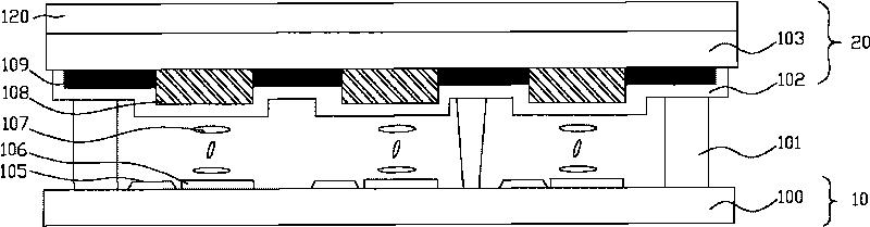
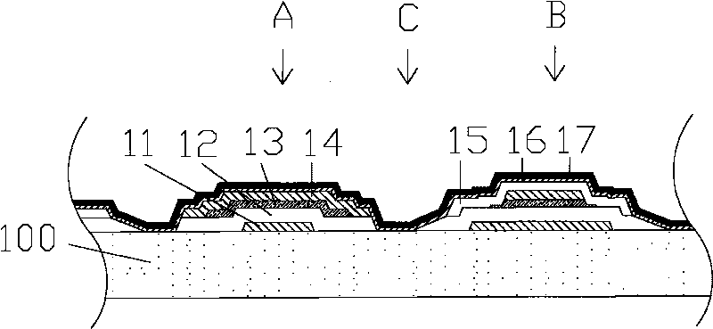
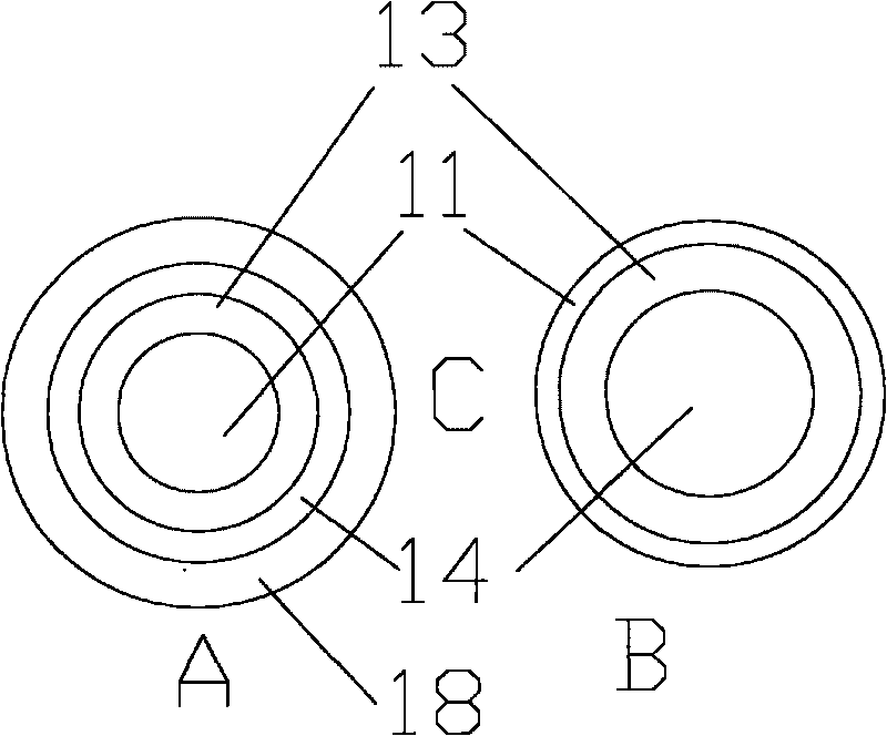
[0037] In order to make the above-mentioned objects, features and advantages of the present invention more obvious and understandable, the specific embodiments of the present invention will be described in detail below with reference to the accompanying drawings.

[0038] In the following description, many specific details are set forth in order to fully understand the present invention, but the present invention can also be implemented in other ways different from those described herein, so the present invention is not limited by the specific embodiments disclosed below.

[0039] Secondly, the present invention will be described in detail in conjunction with schematic diagrams. In detailing the embodiments of the present invention, for ease of description, the cross-sectional view showing the device structure will not be partially enlarged according to the general scale, and the schematic diagram is only an example, which should not be limited here. The scope of protection of the p...


PUM


Abstract

The invention provides a liquid crystal display device and a manufacturing method thereof. The liquid crystal display device comprises a first substrate, a second substrate and a liquid crystal layer which is clamped between the first substrate and the second substrate. One side, facing the liquid crystal layer, of the first substrate is provided with a functional film layer, wherein a plurality of bosses and / or a plurality of recesses are formed in the functional film layer. The functional film layer comprises one of or a combination of at least two of a gate metal layer, a gate insulation layer, a semiconductor layer, a source drain metal layer and an insulated protection layer. The liquid crystal display device and the manufacturing method thereof can avoid single-angle specular reflection of a smooth plane so as to improve reflectivity of diffuse reflection and enlarge visual angle of reflection. Meanwhile, compared with technology of enhancing backlight intensity, the manufacturing method has the advantages of capacity of meeting the requirement on excellent visibility during indoor and outdoor use without increasing the whole power consumption of the liquid crystal display.

Description

Technical field [0001] The invention relates to the field of flat panel display technology, in particular to a liquid crystal display device and a manufacturing method thereof. Background technique [0002] Liquid crystal display (LCD), as a flat panel display, has many advantages such as clear and precise images, thin thickness, light weight, no radiation, low energy consumption, and low working voltage. It has been widely used in various fields. Generally, a liquid crystal display has two substrates containing electrodes and a liquid crystal layer disposed between the two substrates. The electrodes on the two substrates control the intensity of the electric field applied to the liquid crystal layer to control the deflection of liquid crystal molecules, thereby adjusting the incident light Transmittance, in order to realize the control of the brightness and darkness of the display pixels. [0003] Thin Film Transistor (TFT) liquid crystal displays are increasingly used in modern ...

Claims


Application Information

Patent Timeline
Patent Type & Authority Applications(China)
IPC IPC(8): G02F1/1362G02F1/1368H01L21/82
Inventor 胡君文李林洪胜宝谢凡王磊何基强
Owner TRULY SEMICON
Features
  • R&D
  • Intellectual Property
  • Life Sciences
  • Materials
  • Tech Scout
  • Unparalleled Data Quality
  • Higher Quality Content
  • 60% Fewer Hallucinations
Learn More