Removal method of water vapor on crystal wafer surface

A chip and water vapor technology, which is applied in the direction of electrical components, semiconductor/solid-state device manufacturing, circuits, etc., can solve the problem of incomplete water vapor removal, and achieve the effect of uniformity improvement and wide temperature range

Active Publication Date: 2013-01-30
SHANGHAI HUAHONG GRACE SEMICON MFG CORP
View PDF0 Cites 2 Cited by
  • Summary
  • Abstract
  • Description
  • Claims
  • Application Information

AI Technical Summary

Problems solved by technology

[0005] In order to solve the problem of incomplete removal of water vapor on the surface of the silicon companion in the prior art, the present invention provides a method for completely removing the water vapor adsorbed on the surface of the silicon companion, and achieves the purpose of improving the thickness uniformity of the silicon dioxide film

Method used


Image

  • Removal method of water vapor on crystal wafer surface

Examples


Embodiment Construction

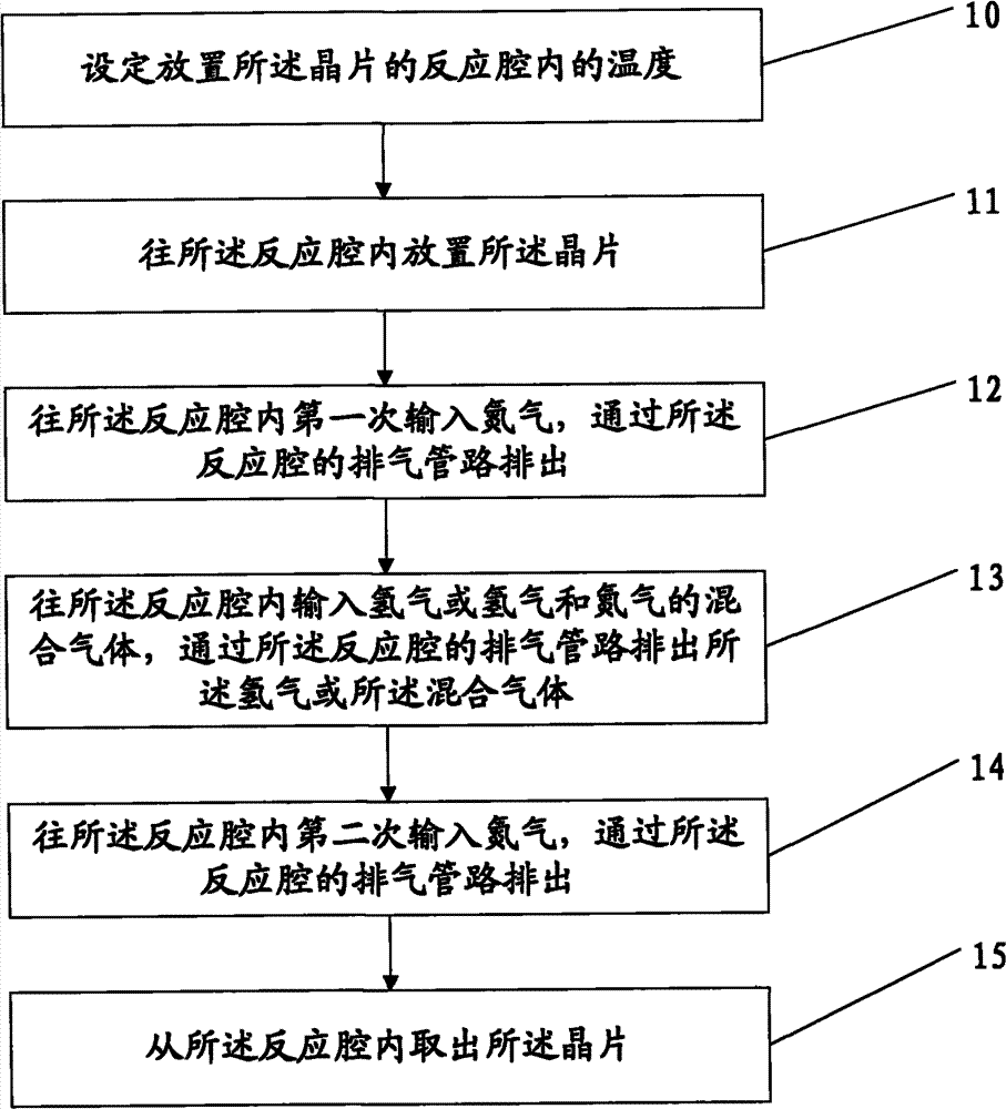
[0015] First, please refer to figure 1 , figure 1 It is a flowchart of a method for removing water vapor from the surface of a wafer of the present invention. As can be seen from the figure, the present invention includes the following steps: Step 10: Setting the temperature in the reaction chamber where the wafer is placed, the temperature in the reaction chamber The range is 400 degrees Celsius to 800 degrees Celsius, preferably, the temperature in the reaction chamber is 500 degrees Celsius; Step 11: Place the wafer in the reaction chamber, and the wafers placed in the reaction chamber are generally placed in a quartz boat and then placed in the reaction chamber; step 12: input nitrogen into the reaction chamber for the first time, and discharge it through the exhaust pipe of the reaction chamber. The time for the first nitrogen input is 5 minutes, and the input The nitrogen gas is 20 liters; step 13: input hydrogen or the mixed gas of hydrogen and nitrogen into the reacti...


PUM


Abstract

The invention provides a removal method of water vapor on the crystal wafer surface, comprising the following steps of setting the temperature of a reaction cavity which is set for containing a crystal wafer; putting the crystal wafer in the reaction cavity; inputting nitrogen into the reaction cavity for the first time and exhausting the nitrogen through an exhaust pipeline of the reaction cavity; inputting hydrogen or mixed gas of the hydrogen and the nitrogen into the reaction cavity and exhausting the hydrogen or the mixed gas of the hydrogen and the nitrogen through the exhaust pipeline of the reaction cavity; inputting the nitrogen into the reaction cavity for the second time and exhausting the nitrogen through the exhaust pipeline of the reaction cavity; and taking out the crystal wafer from the reaction cavity. In the invention, nitrogen used in the prior art is replaced with hydrogen so as to completely remove the water vapor on the crystal wafer surface. When being used as an accompany film in a silicon dioxide diaphragm growth technology, the crystal wafer can obviously improve the uniformity of the thickness of a silicon dioxide diaphragm. In addition, the use of hydrogen is also beneficial to removing the water vapor adsorbed on the inner surface of the reaction cavity.

Description

technical field [0001] The invention relates to a film growth process in the field of semiconductors, in particular to a method for removing water vapor on the surface of a wafer. Background technique [0002] Silicon dioxide film is a very important film in semiconductor devices, which can be used as gate oxide layer, gate side selective oxide layer and buffer oxide layer. Silicon dioxide film growth is carried out in the reaction chamber, and requires a silicon companion. A typical reaction chamber can hold up to 170 wafers, of which 150 are product wafers, and 20 are silicon accompanying wafers placed at both ends of the product wafer. If there are less than 150 product wafers, additional silicon companion wafers need to be loaded until it is full. Therefore, in each growth process, a large number of silicon companion wafers are required. The surface of the silicon wafer must be clean, the most important of which is the control of water vapor. [0003] As the critical...

Claims


Application Information

Patent Timeline
Patent Type & Authority Patents(China)
IPC IPC(8): H01L21/00H01L21/31
Inventor 许忠义张永福
Owner SHANGHAI HUAHONG GRACE SEMICON MFG CORP
Why Eureka
Try Eureka