Method for manufacturing integrated packaged high-power LED illuminating light source, and LED illuminating lamp

A LED lighting, LED lighting technology, applied in light source, electric light source, point light source, etc., can solve the problems of light source glare and light pollution, large chemical radiation, unnatural light, etc., achieve soft light, high color rendering, The effect of convenient transportation and installation

Inactive Publication Date: 2010-06-16
赵翼
View PDF0 Cites 6 Cited by
  • Summary
  • Abstract
  • Description
  • Claims
  • Application Information

AI Technical Summary

Problems solved by technology

[0003] The manufacturing method of the integrated package high-power LED lighting source provided by the present invention and the LED lighting lamp are to overcome glare and light pollution caused by

Method used


Image

  • Method for manufacturing integrated packaged high-power LED illuminating light source, and LED illuminating lamp
  • Method for manufacturing integrated packaged high-power LED illuminating light source, and LED illuminating lamp
  • Method for manufacturing integrated packaged high-power LED illuminating light source, and LED illuminating lamp

Examples


Embodiment

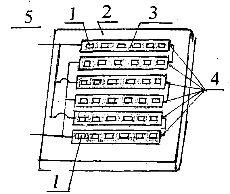
[0014] Example: see Figure 1-Figure 5 ,

[0015] This embodiment integrates a manufacturing method of encapsulating a high-power LED lighting source, and the LED lighting source is used for a high-power street lamp. The preparation method comprises the following steps:

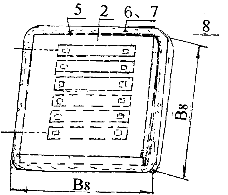
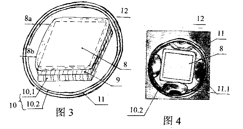
[0016] 1) see figure 1 , select six single white LED chips 1 belonging to semiconductor elements, put them on the substrate 2 made of organic materials according to a certain distance, and use conductive gel silver glue 3 to bond and fix the six single white LED chips to form a light emitting chip 4 ; The power of a single white LED chip 1 is 0.01-3 watts (can be purchased in companies specializing in the production of semiconductor-LED chips in the world). 2) see figure 1 (For example), six light-emitting chips 4 are connected in series (two in series) and parallel (three in parallel) to achieve the light source chip 5 with a required power of 90 watts. 3) see figure 2 1. The light source chip 5 and ...


PUM

PropertyMeasurementUnit
Side lengthaaaaaaaaaa

Abstract

The invention relates to a method for manufacturing an integrated packaged high-power LED illuminating light source and an LED illuminating lamp. The manufacturing method comprises the following steps: (1) selecting a plurality of single white light LED wafers, putting the wafers on a substrate, and bonding the wafers into light-emitting chips by fulmargin; (2) connecting more than one light-emitting chips in series or/and in parallel to form a light source chip when reaching required power; (3) mixing the light source chip, substrate used epoxy resin glue, scattering agent and fluorescent powder for integral packaging; and (4) adhering the integrally packaged chips on a base plate and also arranging the integrally packaged chips on a heat radiator so as to arrange the combined components inside a lampshade to form the high-power LED illuminating light source, and then connecting the high-power LED illuminating light source with a control circuit to arrange the combined components inside a lamp casing to form the high-power LED illuminating lamp. The method for manufacturing the integrated packaged high-power LED illuminating light source and the LED illuminating lamp are characterized in that compared with existing LED multi-light spot illuminating light sources formed by connecting light spots which are separately packaged with single small lamp beads in series and in parallel, only one tenth packaging material is required; the light rays of the lamp is clear and soft and similar to natural daylight; the lamp has the advantages of uniform light emitting, no glare, no light pollution, no radiation, visual fatigue prevention and slow attenuation (less than 5 percent within three years); and compared with traditional incandescent lamps, sodium lamps and energy-saving lamps, the LED illuminating lamp also has the advantages of energy saving, long service life, environmental protection, high safety, solid state packaging, convenient transportation, and the like.

Description

[0001] (1) Technical field: the present invention relates to a method for manufacturing an LED lighting source used for lamps and an LED lighting lamp. It belongs to the category of lighting device parts (F21V). (two) background technology: [0002] LED lighting has become a lighting development trend. Compared with traditional lighting incandescent lamps, sodium lamps, and energy-saving lamps, LED lighting has the following advantages: energy saving, long life, environmental protection and safety, healthy light sources, large voltage fluctuations, and convenient use. At present, the commonly used LED lighting systems are all using commercially available small lamp pearl points that are individually packaged into single grains, and each of them is connected in series and parallel to make the lighting source of the required power. The power of this LED light source is low, and the maximum can only be 2 Watts, equivalent to 20 watts of incandescent lamps, basically meet the requ...

Claims


Application Information

Patent Timeline
IPC IPC(8): F21S2/00F21V9/10F21V19/00F21V23/00F21V29/00H01L25/075H01L33/48H01L33/50F21Y101/02F21V9/40
CPCH01L33/52F21K9/90H01L25/0753F21Y2101/02F21Y2115/10H01L2924/0002H01L2924/00
Inventor 李远清
Owner 赵翼
Why Eureka
Try Eureka