Cleaning device for semiconductor base material

A cleaning device, semiconductor technology, applied in the direction of liquid cleaning method, semiconductor/solid-state device manufacturing, cleaning method and utensils, etc., can solve the problems of cracked edge of mask R, unsafe, difficult adhesion of particles or pollutants, etc.

Active Publication Date: 2010-06-16
GUDENG PRECISION IND CO LTD
View PDF0 Cites 3 Cited by
  • Summary
  • Abstract
  • Description
  • Claims
  • Application Information

AI Technical Summary

Problems solved by technology

However, the area of ​​the sprayed water flow or air flow of such nozzle 130 is limited. Obviously, it takes a long time to clean only one surface of the mask R, and when the other surface of the mask R is to be cleaned, It is time-consuming and unsafe to turn over the mask R again, fix it and clean it aga

Method used


Image

  • Cleaning device for semiconductor base material
  • Cleaning device for semiconductor base material
  • Cleaning device for semiconductor base material

Examples


Embodiment Construction

[0046] Although the preferred embodiments of the present invention are disclosed below, they are not intended to limit the present invention. Any person familiar with the similar art can make some changes and modifications without departing from the spirit and scope of the present invention. Therefore, the present invention The scope of patent protection shall be defined by the scope of patent application attached to this specification.

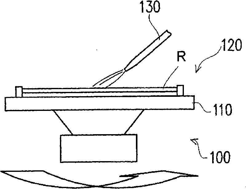
[0047] First, please refer to figure 2 , is a general view of a cleaning device of the present invention.

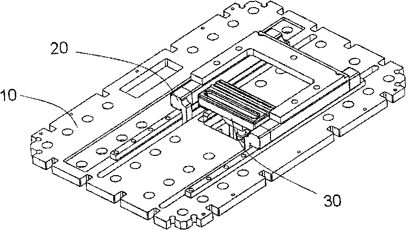
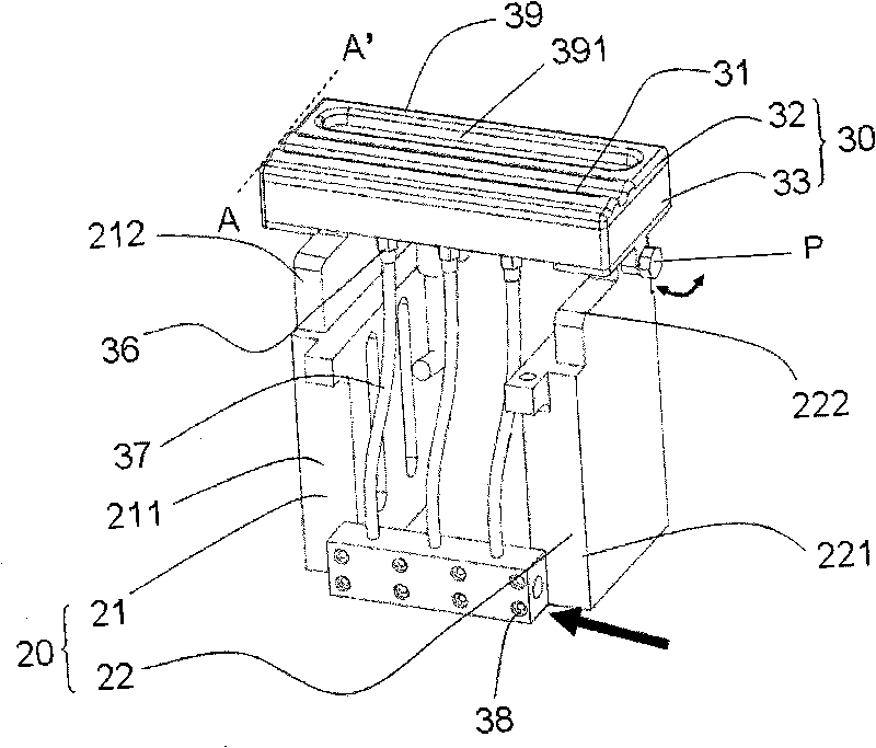
[0048] Next, please refer to image 3 , is a general view of the base and the movable cleaning unit of the cleaning device of the present invention. The cleaning device of the present invention is used to clean semiconductor substrates or masks. This cleaning device at least includes a working platform 10, a base 20 and a movable cleaning unit 30. The above-mentioned base 20 is composed of two mutually parallel The vertical substrat...


PUM


Abstract

The invention discloses a cleaning device for semiconductor base material, in particular to a device for removing pollutant from the semiconductor base material and the surface of a mask in the semiconductor process. The cleaning device comprises a working platform, a base and a movable cleaning unit, wherein the base comprises two parallel vertical base plates, each vertical base plate is provided with a bottom end and a top end, and the bottom end of each vertical base plate is arranged on the working platform; and the movable cleaning unit is pivoted at the tops of the two vertical base plates of the base. The movable cleaning unit is at least provided with a slender outlet which is used for delivering a fluid to the semiconductor base material or the surface of the mask.

Description

technical field [0001] The invention relates to a semiconductor substrate cleaning device and a mask cleaning device, in particular to a device for removing pollutants from the semiconductor substrate and the surface of a mask in a semiconductor process. Background technique [0002] In semiconductor processing, cleaning of semiconductor substrates or masks is an important step. When cleaning, it is necessary to efficiently and thoroughly clean the organic substances, pollutants, chemical residues, etc. remaining on the surface of the semiconductor substrate or mask, otherwise the contaminated mask will cause poor product quality in the subsequent process. Serious loss of yield. [0003] Please refer to figure 1 Shown is a schematic side view of a conventional mask cleaning device. The mask cleaning device 100 fixes the mask R through a horizontal mask fixing unit 120 arranged on the rotating platform 110, and then passes through a movable cleaning nozzle 130 to generate ...

Claims


Application Information

Patent Timeline
IPC IPC(8): H01L21/00H01L21/02G03F1/00B08B3/02G03F1/82
Inventor 潘勇顺
Owner GUDENG PRECISION IND CO LTD
Why Eureka
Try Eureka