Interlayer dielectric layer, interconnection structure and manufacturing method thereof

A technology of an interlayer dielectric layer and a manufacturing method, which is applied to the interconnection structure and its manufacturing, and the field of the interlayer dielectric layer, can solve the problems of increased reflection and scattering, easy cracking, and large stress, and achieves reduced reflection and scattering. Not easy to crack, simple structure

Inactive Publication Date: 2012-12-12
SEMICON MFG INT (SHANGHAI) CORP +1
View PDF1 Cites 0 Cited by
  • Summary
  • Abstract
  • Description
  • Claims
  • Application Information

AI Technical Summary

Problems solved by technology

[0009] In the above technical solution, the interlayer dielectric layer adopts a fluorine-doped oxide layer 207b. Since the fluorine in the fluorine-doped oxide is easy to diffuse, it is necessary to add a first oxide layer 204 in between for isolation. At the same time, it is necessary to grow a second The tetroxide layer 208 is used to isolate and repair defects, so that too many and too thick interlayer dielectric layers are formed, resulting in increased production costs and complicated processes. At the same time, due to the large number of stacked layers, the stress between layers is caused. Larger, easy to crack, and the reflection and scattering of light between layers increases, and the transmittance is low

Method used


Image

  • Interlayer dielectric layer, interconnection structure and manufacturing method thereof
  • Interlayer dielectric layer, interconnection structure and manufacturing method thereof
  • Interlayer dielectric layer, interconnection structure and manufacturing method thereof

Examples


Embodiment Construction

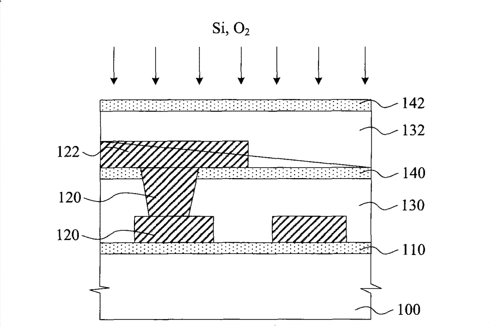
[0032] The interlayer dielectric layer of the present invention adopts a fluorine-free dielectric layer, which avoids the easy diffusion of fluorine in the fluorine-containing oxide of the prior art, and does not need to add a first oxide layer for isolation and a fourth oxide layer in between. To repair defects, the number of interlayer dielectric layers formed is small, the structure is simple, and the cost is low; the reflection and scattering of light between layers are reduced, and the transmittance is high; and because of the small number of layers, the interlayer The stress is small, and it is not easy to cause cracking.

[0033]Below by describing specific embodiment in detail according to accompanying drawing, above-mentioned object and advantage of the present invention will be clearer:

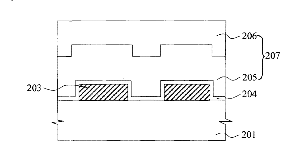
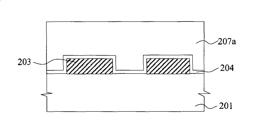
[0034] refer to Figure 6 , the present invention firstly provides a method for manufacturing an interlayer dielectric layer in a CMOS image sensor, comprising: providing a semicon...


PUM


Abstract

The invention discloses an interlayer dielectric layer, an interconnection structure and a manufacturing method thereof. The manufacturing method of the interlayer dielectric layer in a complementary metal-oxide semiconductor (CMOS) image sensor comprises the following steps of: providing a semiconductor substrate; forming a dielectric layer on the semiconductor substrate; reducing the thickness of the dielectric layer to a preset thickness; and forming a second dielectric layer and an anti-reflection layer on the thinned dielectric layer, wherein the dielectric layer does not contain fluorine. In the invention, the dielectric layer without fluorine is adopted for the interlayer dielectric layer, the diffusion of the fluorine of the fluorine-containing oxide in the prior art is avoided, and a first oxide layer for separation and a fourth oxide layer for repairing defects are unnecessary to add. The invention has advantages of less interlayer dielectric layers, simple structure, low cost, reduction of the light reflection and dispersion among layers and high transmittance. In addition, due to few layers, the stress among the layers is little, and cracking can not easily casued.

Description

technical field [0001] The invention relates to the technical field of semiconductors, in particular to an interlayer dielectric layer in a CMOS image sensor, an interconnection structure and a manufacturing method thereof. Background technique [0002] In the semiconductor industry, interconnect structures are used to provide wiring between devices on an IC chip and the entire package. In this technology, devices such as field-effect transistors (FETs) are first formed on the surface of a semiconductor substrate, and then The interconnect structure is formed in the back-end-of-line (BEOL) process. Typical interconnect structures include at least one dielectric material into which are embedded metal patterns in the form of vias and / or lines. [0003] The prior art discloses a back-end process of a semiconductor device, referring to figure 1 As shown, it includes: providing a semiconductor substrate 100, a device layer is formed in the semiconductor substrate, and an undope...

Claims


Application Information

Patent Timeline
Patent Type & Authority Patents(China)
IPC IPC(8): H01L21/768H01L21/316H01L27/146H01L23/532
Inventor 程永亮王娉婷高关且杨承朱虹吴金刚
Owner SEMICON MFG INT (SHANGHAI) CORP
Why Eureka
Try Eureka