Field effect transistor device using carbon nano tube as electrode and preparation method thereof

A field effect transistor and carbon nanotube technology, which is applied in the field of field effect transistor devices and their preparation to achieve the effects of high application value and high response sensitivity

Inactive Publication Date: 2010-06-16
PEKING UNIV
View PDF0 Cites 7 Cited by
  • Summary
  • Abstract
  • Description
  • Claims
  • Application Information

AI Technical Summary

Benefits of technology

This patented technology allows for creation of highly sensitive electronic components that are able to respond quickly even when exposed to different types or levels of stress (temperature). These materials have potential applications in both chemicals and biological systems due their ability to detect changes caused by small amounts of pressure applied during use on surfaces.

Problems solved by technology

Technological Problem: The technical problem addressed in this patented study relating to improving the function of moleculum tubular membranes made from single wall carbon nanostructures such as quantum dots, while also addressing issues related to manufacturing processability, sensitivity, durability, and functionality of these films.

Method used


Image

  • Field effect transistor device using carbon nano tube as electrode and preparation method thereof
  • Field effect transistor device using carbon nano tube as electrode and preparation method thereof
  • Field effect transistor device using carbon nano tube as electrode and preparation method thereof

Examples


Embodiment 1

[0030] Embodiment 1, preparation carbon nanotube transistor device

[0031] The preparation method of the carbon nanotube transistor device includes the following steps in sequence:

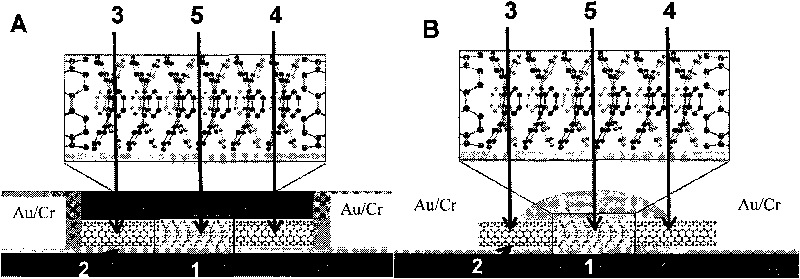
[0032] 1) Mesoporous SiO doped with CoMo 2 Particles act as a catalyst that is uniformly distributed on SiO on the surface of a heavily doped silicon substrate 2 layer; the SiO 2 The layer is grown on the silicon wafer by the thermal evaporation method with a thickness of 300nm; using ethanol as the carbon source, using the CVD method on SiO 2 A layer of single-walled carbon nanotubes is obtained on top of the layer. The single-walled carbon nanotube layer is located in the center of the silicon substrate.

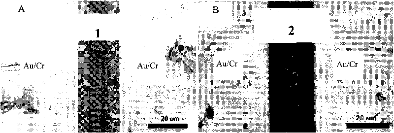
[0033] Afterwards, a metal mask is covered on the single-walled carbon nanotube layer, and a Cr layer and an Au layer are sequentially obtained by using a thermal evaporation method, and Au / Cr is used as a source region and a drain region of the carbon nanotube transistor device. Wherein...

Embodiment 2

[0042] Embodiment 2, preparation carbon nanotube transistor device

[0043] The preparation method of the carbon nanotube transistor device includes the following steps in sequence:

[0044] 1) Mesoporous SiO doped with CoMo 2 Particles act as a catalyst that is uniformly distributed on SiO on the surface of a heavily doped silicon substrate 2 layer; the SiO 2 The layer is grown on the silicon wafer by the thermal evaporation method with a thickness of 300nm; using ethanol as the carbon source, using the CVD method on SiO 2 A layer of single-walled carbon nanotubes is obtained on top of the layer. The single-walled carbon nanotube layer is located in the center of the silicon substrate.

[0045] Afterwards, a metal mask is covered on the single-walled carbon nanotube layer, and a Cr layer and an Au layer are sequentially obtained by using a thermal evaporation method, and Au / Cr is used as a source region and a drain region of the carbon nanotube transistor device. Wherein...

Embodiment 3

[0054] Embodiment 3, preparation carbon nanotube transistor device

[0055] 1) Mesoporous SiO doped with CoMo 2 Particles act as a catalyst that is uniformly distributed on SiO on the surface of a heavily doped silicon substrate 2 layer; the SiO 2 The layer is grown on the silicon wafer by the thermal evaporation method with a thickness of 300nm; using ethanol as the carbon source, using the CVD method on SiO 2 A layer of single-walled carbon nanotubes is obtained on top of the layer. The single-walled carbon nanotube layer is located in the center of the silicon substrate.

[0056] Afterwards, a metal mask is covered on the single-walled carbon nanotube layer, and a Cr layer and an Au layer are sequentially obtained by using a thermal evaporation method, and Au / Cr is used as a source region and a drain region of the carbon nanotube transistor device. Wherein, the distance between the two electrodes is 20 μm, the thickness of the Cr layer is 5 nm, and the thickness of the ...


PUM

PropertyMeasurementUnit
Thicknessaaaaaaaaaa
Widthaaaaaaaaaa
Widthaaaaaaaaaa

Abstract

The invention provides a field effect transistor device using a carbon nano tube as an electrode and a preparation method thereof. In the device, the materials forming a source region and a drain region are at least one single-walled carbon nano tube respectively, and the materials forming a channel region are various organic semi-conductor molecules. The preparation method is as follows: by adopting a method combining a device manufacturing process from top to bottom with a molecule self-assembly method from bottom to up, functional molecules are introduced in a functional molecule transistor device. By adopting a one-dimensional trajectory single-walled carbon nano tube as a point contact body and introducing the hexabenzocoronene compound with a self-assembly characteristic, the nano field effect transistor of high performance can be obtained which has high response sensitivity to various outside stimuli. The carbon nano tube transistor device has very high application value in terms of ultrasensitive environmental stimuli response devices, ultrasensitive solar stimuli response devices and the like. The device plays an essential role in promoting the development of ultramicro photoelectric devices with various dimensions at molecular level.

Description


Claims


Application Information

Patent Timeline
Owner PEKING UNIV
Why Eureka
Try Eureka