Error correcting controller, flash memory chip system thereof and error correcting method

A technology of error correction and flash memory chip, which is applied in the direction of instruments, static memory, etc., and can solve the problems of unable to support flash memory and error correction ability

Active Publication Date: 2010-06-23
PHISON ELECTRONICS
View PDF0 Cites 0 Cited by
  • Summary
  • Abstract
  • Description
  • Claims
  • Application Information

AI Technical Summary

Problems solved by technology

The error correction capability of the old host controller is often unable to support the error correction capability required by the new generation of flash memory (for example, when the old host controller is produced, it is only equipped with the ability to detect 2 error bits / error correct 1 error bit However, when the new flash requires a controller capable of error correcting 4 error bits to function properly), this old host controller will not be able to support the new generation of flash memory

Method used


Image

  • Error correcting controller, flash memory chip system thereof and error correcting method
  • Error correcting controller, flash memory chip system thereof and error correcting method
  • Error correcting controller, flash memory chip system thereof and error correcting method

Examples


no. 1 example

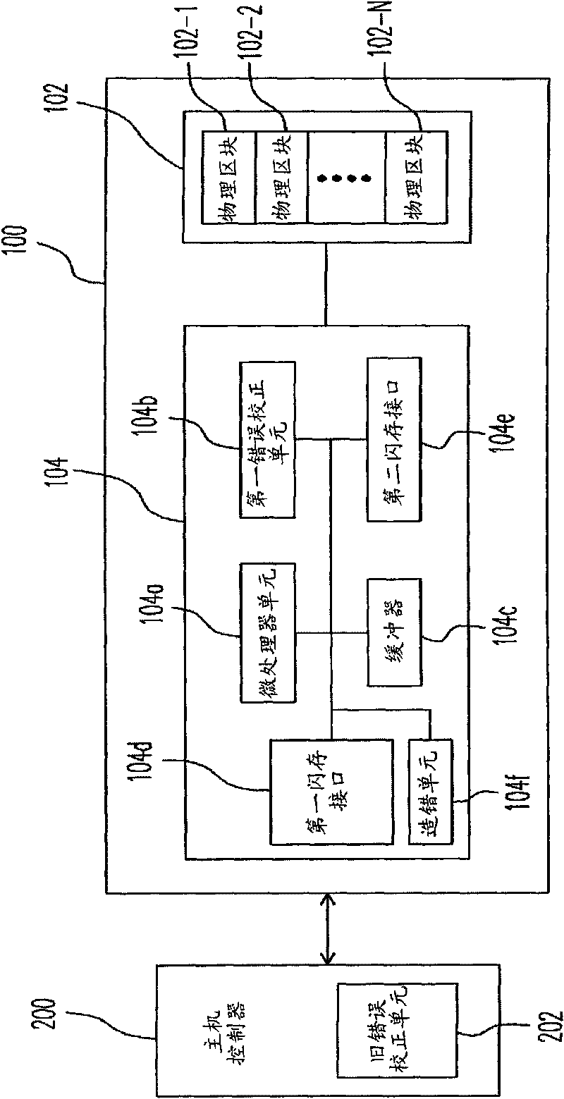
[0061] figure 1 is a schematic block diagram illustrating a flash memory chip system according to the first embodiment of the present invention.

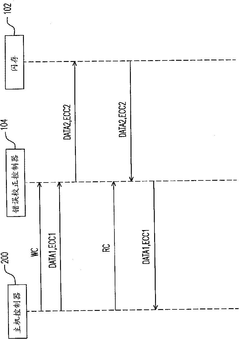
[0062] Please refer to figure 1 , the flash chip system 100 includes a flash memory 102 and an error correction controller 104 . The flash memory chip system 100 is connected with the host controller 200, and the host controller 200 performs various access operations on it. In particular, the host controller 200 has an old error correction unit 202, wherein the old error correction unit 202 can provide the ability to correct 1 error bit and detect 2 error bits for data. It is worth mentioning that in this embodiment, the flash memory 102 and the error correction controller 104 are packaged as a single system chip, but in another embodiment of the present invention, the flash memory 102 and the error correction controller 104 can be independent chips.

[0063] The flash memory 102 is a storage medium for storing data. The flash m...

no. 2 example

[0095] Figure 4 is a schematic block diagram illustrating a flash memory chip system according to a second embodiment of the present invention.

[0096] Please refer to Figure 4 , the flash chip system 400 includes a flash memory 402 and an error correction controller 404 . The flash chip system 400 is connected to the host controller 200 so that the host controller 200 can perform various access operations thereon. As mentioned above, the host controller 200 has the old error correction unit 202, wherein the old error correction unit 202 can provide the capability of error correction of 1 error bit and detection of 2 error bits for data.

[0097] The flash memory 402 is the same as the flash memory 102 in the first embodiment, and will not be repeated here.

[0098]The error correction controller 404 is electrically connected to the flash memory 402 and used for executing error correction codes and error correction programs that meet the error correction capability requi...


PUM


Abstract

The invention relates to an error correcting controller that is connected between an old host controller with a low-order error correction function and a new flash memory with a high-order error correcting function. When the old host controller is to write data and old error correcting coding to the new flash memory, the error connecting controller generates new error correcting coding with the high-order error correcting function. Then, when the host controller is to read data and old error correcting coding from the new flash memory, the error correcting controller performs the error correcting procedure based on the new error correcting coding and transmits corresponding data based on the error correcting result and the error correcting ability of the old host controller. Accordingly, the invention ensures that the old host controller accesses the new flash memory without altering the framework of the old host controller.

Description

technical field [0001] The present invention relates to a flash memory chip system, and in particular to a flash memory chip system with error correcting function, its error correction controller and error correction method. Background technique [0002] Digital cameras, mobile phones, and MP3 players have grown rapidly in recent years, making consumers' demand for storage media also increase rapidly. Because flash memory (Flash Memory) has the characteristics of data non-volatility, power saving, small size and no mechanical structure, it is suitable for portable applications, and is most suitable for such portable products powered by batteries. For example, a memory card is a storage device using NAND flash memory as a storage medium, and has been widely used as a storage medium in digital cameras, mobile phones and MP3 players. [0003] Since NAND flash memory has the characteristics of writing data in units of pages and erasing data in units of blocks, each storage unit...

Claims


Application Information

Patent Timeline
Patent Type & Authority Applications(China)
IPC IPC(8): G11C29/44
Inventor 郑国义梁立群朱健华
Owner PHISON ELECTRONICS
Why Eureka
Try Eureka