Air sucking device and semiconductor processing device

A technology of air extraction device and processing device, which is used in semiconductor/solid-state device manufacturing, electrical components, gaseous chemical plating, etc., can solve the problems of complex maintenance and operation, low efficiency, etc. Effect

Active Publication Date: 2011-09-14
BEIJING NAURA MICROELECTRONICS EQUIP CO LTD
View PDF0 Cites 0 Cited by
  • Summary
  • Abstract
  • Description
  • Claims
  • Application Information

AI Technical Summary

Problems solved by technology

[0006] When there is a problem with the lower electrode and maintenance and operation are required, the entire device must be opened and exposed to the atmosphere, which is complicated and inefficient

Method used


Image

  • Air sucking device and semiconductor processing device
  • Air sucking device and semiconductor processing device
  • Air sucking device and semiconductor processing device

Examples


specific Embodiment

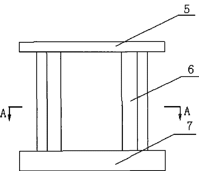
[0023] Such as image 3 — Figure 6 As shown, the air extraction device is a cylindrical structure with a cavity 9 inside, and the side wall 6 of the cylindrical structure is provided with 3 openings 10 and 3 gas passages 8, 3 openings 10 and 3 gas passages 8 spaced apart from each other. In fact, three fan-shaped side walls that are evenly distributed along the circumference of the circular cylinder are dug out, and the remaining side walls are made into a hollow structure.

[0024] The upper and lower ends of the cylinder are provided with connecting flanges 5 and 7, and ring-shaped sealing grooves and bolt mounting holes can be respectively provided on the top of the upper flange 5 and below the lower flange, so that it is convenient to connect with other equipment and ensure sealing etc.

[0025] The lower end flange 7 may be a blind flange, and the middle part of the lower surface of the blind flange is recessed upward to form a uniform flow cavity 11 .

[0026] The p...


PUM


Abstract

The invention discloses an air sucking device and a semiconductor processing device. The air sucking device has a cylindrical structure which is provided with a cavity in the middle, respectively provided with flanges at the upper end and the lower end, and provided with one or more openings on the side wall; a plurality of gas passages are arranged in the side wall along the axial direction; thelower part of the cylindrical structure is provided with uniform stream cavities; and the lower ends of the gas passages are respectively communicated with the uniform stream cavities. After the lower part of a process cavity of a semiconductor processing device is provided with the air sucking device, a lower electrode can be partially placed in the cavity in the middle of the air sucking device, the air suction on the process cavity can be realized by the gas passages in the side wall, and the lower electrode can be maintained and operated by an opening on the side wall. The invention improves the maintenance efficiency and reduces the shutdown time.

Description

technical field [0001] The invention relates to a semiconductor processing technology, in particular to an air extraction device and a semiconductor processing device. Background technique [0002] In the semiconductor manufacturing process, the process chamber usually provides a vacuum environment for the processing of semiconductor wafers. By supplying the reaction gas to the process chamber, under low pressure, the reaction gas passes through the upper electrode and the lower electrode under the excitation of radio frequency power to generate Ionization forms plasma, so that the corresponding material is etched or deposited on the surface of the semiconductor substrate, and the reflected product is separated from the surface of the etched substance, and is pumped out of the process chamber by the vacuum pumping system. For semiconductor substrate processing, the uniformity of the entire substrate surface treatment is an extremely important index of the processing technolo...

Claims


Application Information

Patent Timeline
Patent Type & Authority Patents(China)
IPC IPC(8): H01L21/00C23C14/56C23C16/54F04D19/04H01J37/32B01J3/03
Inventor 刘少锋
Owner BEIJING NAURA MICROELECTRONICS EQUIP CO LTD
Why Eureka
Try Eureka