

A two-translation precision positioning workbench for nanoimprint lithography system
A lithography system and precise positioning technology, applied in the field of micro-operating systems, to achieve micro-feed and precise positioning, eliminate nonlinearity, and compact structure
- Summary
- Abstract
- Description
- Claims
- Application Information
AI Technical Summary
Problems solved by technology
Method used
Image

Examples
Embodiment Construction
[0023]The specific implementation, structure, features and effects provided by the present invention will be described in detail below in conjunction with the accompanying drawings and preferred embodiments.
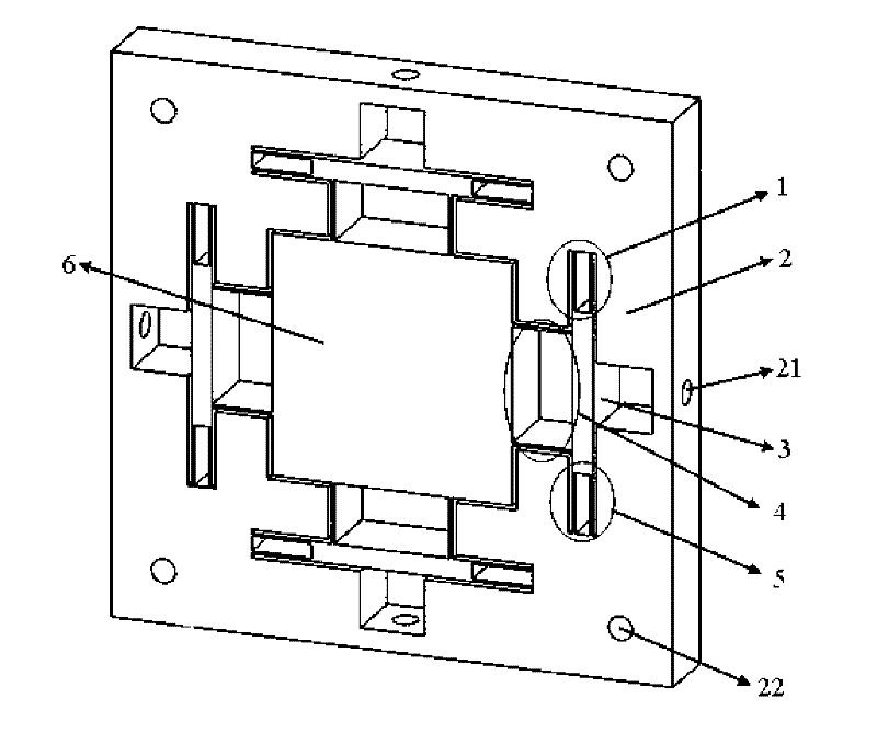
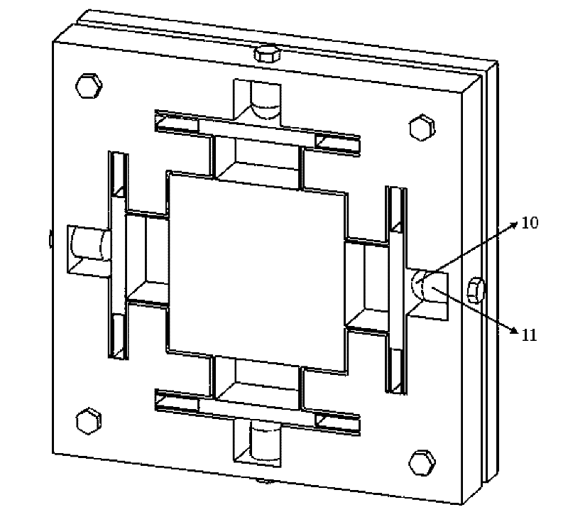
[0024] See Figure 1~4 , a two-translation precision positioning stage for nanoimprint lithography systems. This workbench ( image 3 ) has four piezoelectric ceramic drivers 11, and ball joints 10 are respectively installed on the top, through which the spherical joints 10 are in contact with the moving block 3 in a small-area Hertz contact manner, and the piezoelectric ceramic drivers 11 are placed horizontally, in order to avoid the piezoelectric ceramics from contacting with the moving block 3 The driving link of the flexible mechanism is detached during the working process, and the tail of the piezoelectric ceramic driver 11 is screwed on the base 2 through the holes 21 respectively, and is installed between the driving link of the flexible mechanism and the base i...
PUM
 Abstract
Description
Claims
Application Information