Laminated bottom antireflex structure and etching method

A bottom anti-reflection and bottom anti-reflection layer technology, which is applied in the direction of electrical components, semiconductor/solid-state device manufacturing, circuits, etc., can solve problems such as graphics influence and semiconductor device quality, and achieve the effect of maintaining accuracy

Inactive Publication Date: 2010-07-07
SEMICON MFG INT (SHANGHAI) CORP
View PDF1 Cites 9 Cited by
  • Summary
  • Abstract
  • Description
  • Claims
  • Application Information

AI Technical Summary

Problems solved by technology

When BARCs of different materials are used in combination, this creates a new problem, that is, when etching the lower BARC or other cladding layers under the BARC, the plasma will erode the upper BARC, resulting in damage to the upper layer. The pattern of the BARC will have an impact, and such an impact will be transmitted to the cladding layer under the BARC as the plasma etching progresses, thus affecting the quality of the semiconductor device made

Method used


Image

  • Laminated bottom antireflex structure and etching method
  • Laminated bottom antireflex structure and etching method
  • Laminated bottom antireflex structure and etching method

Examples


Embodiment Construction

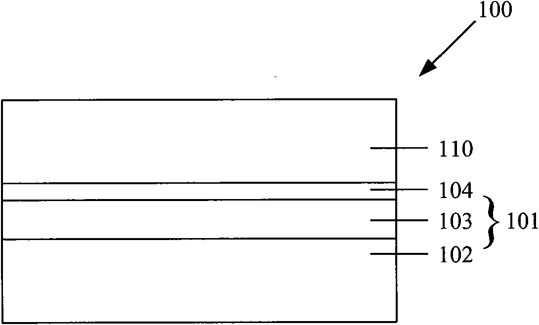
[0024] Such as figure 1 As shown, the specific embodiment provides a laminated structure 100 for photolithography, including a bottom anti-reflection layer 101 and a photoresist layer 110 thereon. The bottom anti-reflection layer 101 is an organic bottom anti-reflection layer 102 with a thickness of about 100 nm. The organic bottom anti-reflection layer 102 is provided with a silicon-containing bottom anti-reflection layer 103 with a thickness of about 50 nm. A silicon oxide layer 104 with a thickness of about 5 nm is also provided on the layer 103. The material forming the organic bottom anti-reflective layer 102 may be an organic anti-reflective material of ODL63 produced by Shin-Etsu Company of Japan. The material for forming the silicon-containing bottom anti-reflective layer 103 may be a silicon-containing anti-reflective material produced by Shin-Etsu Company under the brand name SHB A629.

[0025] The reason for forming the laminated bottom anti-reflective structure 101 w...


PUM

PropertyMeasurementUnit
thicknessaaaaaaaaaa
thicknessaaaaaaaaaa

Abstract

The invention relates to a laminated bottom antireflex structure and an etching method, wherein the laminated bottom antireflex structure comprises an organic bottom antireflex layer and a first layer silicon-containing bottom antireflex layer thereof; and the first layer silicon-contained bottom antireflex layer is also provided with a silicon dioxide layer. Compared with the prior art, the silicon dioxide layer is also arranged on the silicon-contained bottom antireflex layer, and the silicon-contained bottom antireflex layer can be prevented from being damaged when etching the organic bottom antireflex layer, thereby the pattern transfer accuracy can be kept.

Description

Technical field [0001] The invention relates to the field of semiconductor manufacturing, in particular to an anti-reflection structure and an etching method at the bottom of a stack. Background technique [0002] In the manufacturing process of the semiconductor device, the photolithography method of exposing and developing the photoresist is the main method to realize the pattern transfer, which is used to protect the specific area of ​​the processed coating from being etched or doped. With the development of chip technology, the feature pattern size of the chip is getting smaller and smaller, and the material of the cladding layer being processed is becoming more and more diversified. Therefore, during the photolithography exposure process, the photoresist layer and the underlying cladding layer are due to optical The exposure reflection problem caused by the difference in nature has become an important factor affecting the exposure performance. Therefore, it has been difficu...

Claims


Application Information

Patent Timeline
Patent Type & Authority Applications(China)
IPC IPC(8): H01L21/027H01L21/311G03F7/09
Inventor 韩秋华舒强
Owner SEMICON MFG INT (SHANGHAI) CORP
Why Eureka
Try Eureka