Supercharge Your Innovation With Domain-Expert AI Agents!

Method for manufacturing bottom gate type FED lower plate pattern by adopting positive photoresist

A technology of positive photoresist and photoresist, which is applied in cold cathode manufacturing, electrode system manufacturing, discharge tube/lamp manufacturing, etc., and can solve problems such as grid layer 5 short circuit

Inactive Publication Date: 2012-05-09
IRICO
View PDF0 Cites 0 Cited by
  • Summary
  • Abstract
  • Description
  • Claims
  • Application Information

AI Technical Summary

Problems solved by technology

In these methods, since the surface of the lower plate gate layer 5 has been exposed, it is difficult to avoid the cathode emitter 8 (carbon nanotube CNT) on the surface of the gate layer 5 when making the cathode emitter 8 (carbon nanotube CNT). Scattered accumulation (such as figure 2 ), when the voltage is applied to the three electrodes after packaging, the cathode layer 7 and the gate layer 5 are short-circuited

Method used


Image

  • Method for manufacturing bottom gate type FED lower plate pattern by adopting positive photoresist
  • Method for manufacturing bottom gate type FED lower plate pattern by adopting positive photoresist
  • Method for manufacturing bottom gate type FED lower plate pattern by adopting positive photoresist

Examples


Embodiment 1

[0045] 1) Preparation of photosensitive silver paste:

[0046] The photosensitive silver paste consists of 60 parts by weight of silver monomer, 30 parts by weight of methacrylic resin, 4 parts by weight of photoinitiator 2,4,6-trimethylbenzoylphenylphosphonic acid ethyl ester, 5 parts by weight Parts of 2,2,4-trimethyl-1,3-pentanediol monoisobutyrate and 1 part by weight of polymer dispersant BYK410 are mixed and ground uniformly;

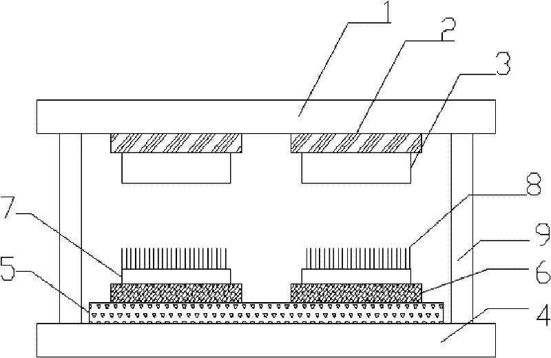
[0047] 2) On the cathode glass substrate 4 after cleaning, use the photosensitive silver paste described in the above step 1) to make the pattern of the gate layer 5 by photolithography;

[0048] The steps of making the gate layer 5 graphics specifically include:

[0049] a). On the cathode glass substrate 4 after cleaning, print a layer of photosensitive silver paste in step 1) to prepare a silver electrode layer;

[0050] b). The substrate in step a) is baked in an oven at a temperature of 95°C for 30 minutes, and then cooled naturally;

[00...

Embodiment 2

[0066] 1) Preparation of photosensitive silver paste:

[0067] The photosensitive silver paste consists of 80 parts by weight of silver monomer, 10 parts by weight of methacrylic resin, 1 part by weight of photoinitiator 2-methyl-1-[4-methylthiophenyl]-2-morpholine Base-1-acetone, 8.5 parts by weight of 2,2,4-trimethyl-1,3 pentanediol monoisobutyrate and 0.5 parts by weight of polymer dispersant BYK180;

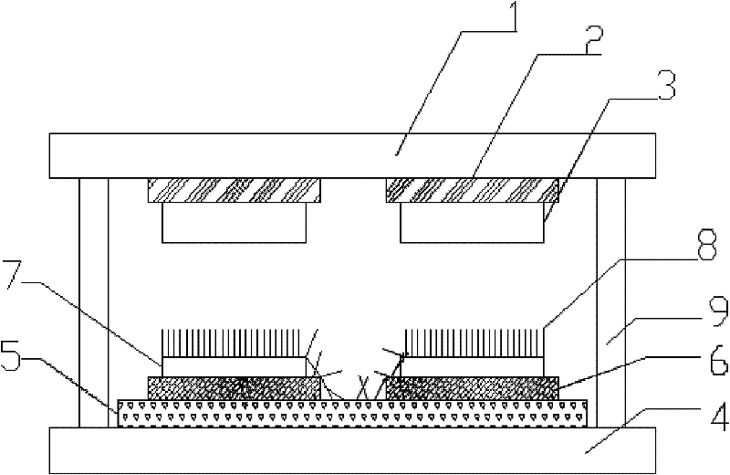
[0068] 2) On the cathode glass substrate 4 after cleaning, use the photosensitive silver paste described in the above step 1) to make the pattern of the gate layer 5 by photolithography;

[0069] The step 2) of making gate layer 5 graphics specifically includes:

[0070] a). On the cathode glass substrate 4 after cleaning, print a layer of photosensitive silver paste in step 1) to prepare a silver electrode layer;

[0071] b). The substrate in step a) is baked in an oven at a temperature of 80°C for 40 minutes, and then cooled naturally;

[0072] c) Use the mask plate of t...

Embodiment 3

[0084] 1) Preparation of photosensitive silver paste:

[0085] The photosensitive silver paste consists of 50 parts by weight of silver monomer, 29 parts by weight of methacrylic resin, 5 parts by weight of photoinitiator 2,4,6-trimethylbenzoylphenylphosphonic acid ethyl ester, 15 parts by weight Parts of 2,2,4-trimethyl-1,3-pentanediol monoisobutyrate and 1 part by weight of polymer dispersant BYK410 are uniformly mixed to form;

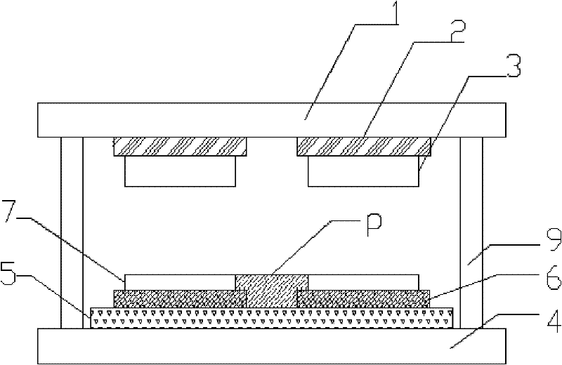
[0086] 2) On the cathode glass substrate 4 after cleaning, use the photosensitive silver paste described in the above step 1) to make the gate layer 5 pattern by photolithography;

[0087] The steps of making the gate layer 5 graphics specifically include:

[0088] a). On the cathode glass substrate 4 after cleaning, print two layers of photosensitive silver paste in step 1) to prepare a silver electrode layer,

[0089] b). The substrate in step a) is baked in an oven at a temperature of 120°C for 10 minutes, and then cooled naturally;

[0090] c...


PUM


Abstract

The invention relates to a method for manufacturing a bottom gate type FED lower plate pattern by adopting positive photoresist for a field emission display. The method comprises the following steps: 1) preparing photosensitive silver paste; 2) manufacturing a gate layer (5) pattern in a cleaned cathode glass substrate (4) by photolithography; 3) manufacturing an insulating material pattern in the gate layer (5) by printing and sintering to obtain a cathode resistance layer (6); 4) using the photosensitive silver paste to manufacture a layer of cathode layer (7) pattern by the photolithography; 5) filling a layer of the positive photoresist (p), exposing and developing under an ultraviolet lamp after drying, thus obtaining a cathode line gap filling pattern p; 6) using electrophoresis, printing and the photolithography to manufacture a cathode emitter (8); and 7) removing the photoresist (p), thus obtaining a complete bottom gate type FED lower substrate structure. The substrate structure made by the method realizes complete insulation of a gate surface and a cathode surface, and solves the problem of short circuit of the gate surface and the cathode surface.

Description

technical field [0001] The present invention relates to the technical field of field emission display manufacture, be specifically related to a kind of Field Emission Display (Field Emission Display; FED) gate layer, dielectric layer, cathode pattern and the fabrication method of the FED lower plate pattern of making emitter on the surface of protection gate . Background technique [0002] In the field emission display of the present invention, electrons are released from the emitter on the cathode emitter material by an electric field to bombard the phosphor on the screen, thereby activating the phosphor to emit light. It is characterized by lightness, thinness, high brightness, wide viewing angle and fast response. [0003] refer to figure 1 Shown is a structural schematic diagram of a field emission display component in the prior art. The structure of the bottom-gate field emission display at least includes an anode and a cathode, and a spacer 9 is arranged between the...

Claims


Application Information

Patent Timeline
Patent Type & Authority Patents(China)
IPC IPC(8): H01J9/00H01J9/02
Inventor 李驰
Owner IRICO
Features
  • R&D
  • Intellectual Property
  • Life Sciences
  • Materials
  • Tech Scout
  • Unparalleled Data Quality
  • Higher Quality Content
  • 60% Fewer Hallucinations
Learn More