Supercharge Your Innovation With Domain-Expert AI Agents!

Method for sealing large-power LED

A LED packaging, high-power technology, applied in the direction of electrical components, circuits, semiconductor devices, etc., can solve the problems of difficulty in finding phosphor silica gel, reduced chip luminous efficiency, shortened LED life, etc., to achieve the effect of increasing luminous efficiency

Inactive Publication Date: 2010-07-21
JIUJIANG LIANHUI OPTOELECTRONICS
View PDF0 Cites 10 Cited by
  • Summary
  • Abstract
  • Description
  • Claims
  • Application Information

AI Technical Summary

Problems solved by technology

[0002] At present, the packaging of high-power LEDs is based on placing the chip on a metal support and coating the fluorescent glue after solidifying the crystal, and then filling it with silica gel and then packaging it into the desired finished shape; the current method of coating the phosphor powder depends on the size of the cup of the support. And it must be fully filled and the filling thickness is large, it is easy to waste a lot of phosphor powder and reduce the luminous efficiency of the chip itself, shortening the life of the LED
If the traditional packaging method is to make the fluorescent silica gel layer thinner and improve the luminous efficiency, but due to the limitation of the phosphor silica gel coating on the die chip, the fluidity of the silica gel will cause the entire phosphor silica gel to be different depending on the form of the bracket. Fluorescent powder evenly spreads on the cup of the overall support, and the phosphor silica gel spread on the surface of the non-actual light-emitting die chip belongs to the wasteful and invalid light-emitting area.
So far, it is difficult to find a high-power LED packaging method that infuses a small amount of phosphor silica gel to increase the light energy of white LEDs.

Method used


Image

  • Method for sealing large-power LED
  • Method for sealing large-power LED
  • Method for sealing large-power LED

Examples


Embodiment Construction

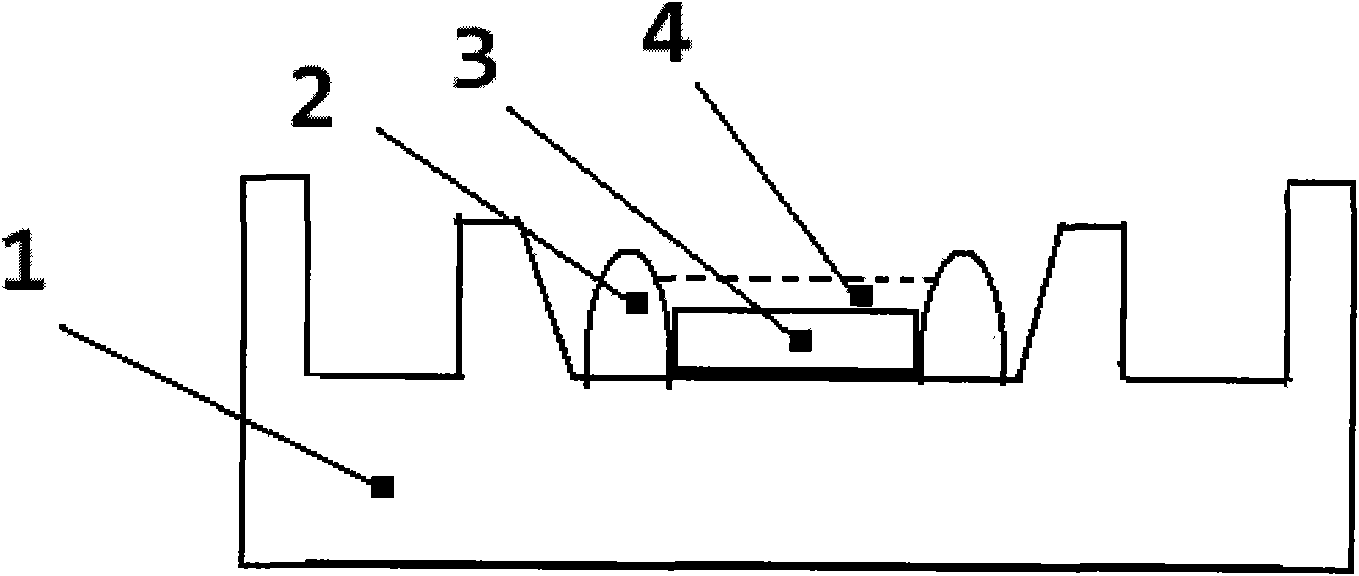
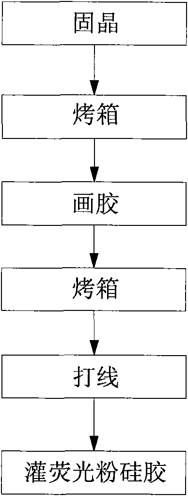
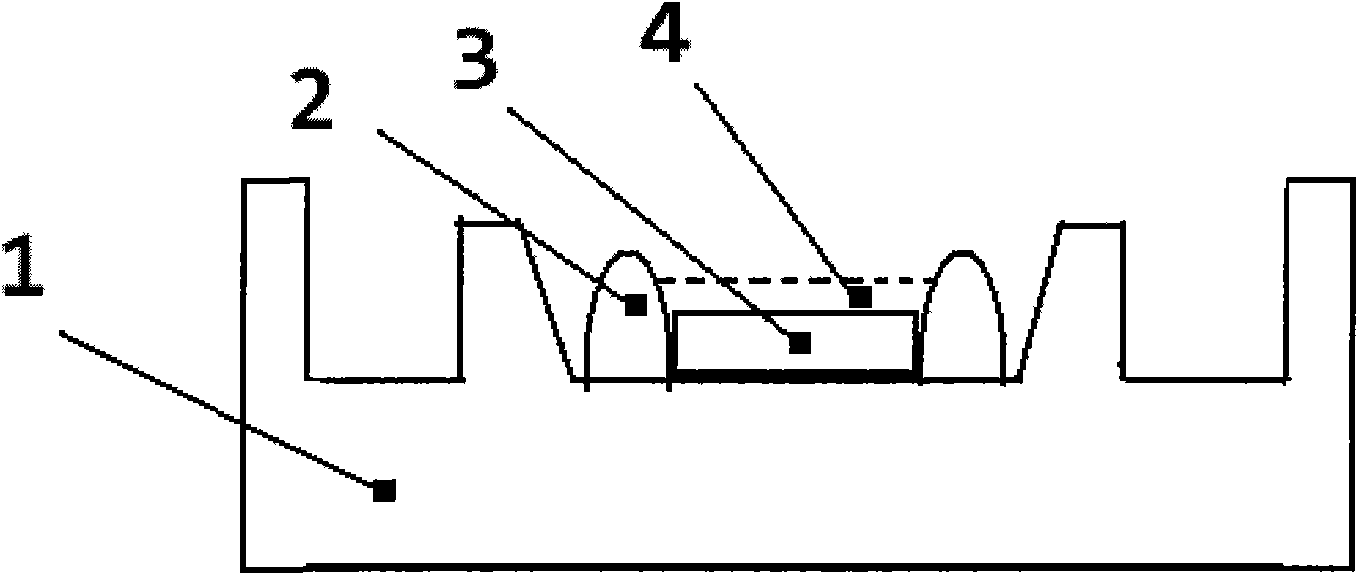
[0017] like Figure 1-2 As shown, a high-power LED packaging method described in the embodiment of the present invention includes the following steps:

[0018] 1) Fixing the LED die chip 3 on the support 1;

[0019] 2) Put the bracket 1 on which the light-emitting diode die chip 3 is fixed into the oven, the temperature of the oven is 120° C., and the curing time is 60 minutes;

[0020] 3) Use a glue dispenser to paint or dispense silica gel with a suitable viscosity coefficient around the LED die chip 3, and coat a layer of silica gel fence 2 around the LED die chip 3. The silica gel fence 2 can be used according to the desired The required thickness of fluorescent powder silica gel 4 is used for single or multiple glue painting and dispensing. When the required thickness is high, the 3D glue painting function can be used to coat the silica gel fence 2 once and then coat the silica gel fence 2 again. The height of the silicone wall 2 is determined according to the thickness...


PUM


Abstract

The invention relates to a method for sealing a large-power LED, comprising the following steps: fixing an LED crystal particle chip on a support; conveying the fixed LED crystal particle chip into an oven; carrying out glue painting or glue dispensing on silica gel with appropriate viscosity coefficient around the LED crystal particle chi p with a glue dispenser; solidifying and then routing a silica gel enclosing wall; and filling a layer of fluorescent powder silica gel in a preset area after completing routing. The invention has the beneficial effects that as the silica gel enclosing wall is coated with silica gel around the LED crystal particle chip, the fluorescent powder silica gel does not flow out of a non-luminous area due to fluid mechanics, so that the fluorescent powder silica gel can be evenly coated on the surface of the actual LED crystal particle chip without wasting the fluorescent powder silica gel and increasing integral luminous efficiency.

Description

technical field [0001] The invention relates to a high-power LED packaging method. Background technique [0002] At present, the packaging of high-power LEDs is based on placing the chip on a metal support and coating the fluorescent glue after solidifying the crystal, and then filling it with silica gel and then packaging it into the desired finished shape; the current method of coating the phosphor powder depends on the size of the cup of the support. And it must be fully filled and the filling thickness is large, which is easy to waste a large amount of phosphor powder and cause the chip itself to reduce the luminous efficiency and shorten the life of the LED. If the traditional packaging method is to make the fluorescent silica gel layer thinner and improve the luminous efficiency, but due to the limitation of the phosphor silica gel coating on the die chip, the fluidity of the silica gel will cause the entire phosphor silica gel to be different depending on the form of ...

Claims


Application Information

Patent Timeline
IPC IPC(8): H01L33/48H01L33/50
Inventor 章炯煜
Owner JIUJIANG LIANHUI OPTOELECTRONICS
Features
  • R&D
  • Intellectual Property
  • Life Sciences
  • Materials
  • Tech Scout
  • Unparalleled Data Quality
  • Higher Quality Content
  • 60% Fewer Hallucinations
Learn More